Kodak compiled a nice market forecast based on data from TSR, Strategies Unlimited, IDG, CDG and also Kodak's own Image Sensor Solution (ISS) group. The data includes both CMOS and CCD sensors:
Interesting to note that DSLR, while being invisible on units chart, represents a good chunk of whole market money in 2009. Sequrity is projected to remain big market all the years through to 2009.
The strange thing is that DSC market goes down with time, both in terms of units and dollars. Probably, it's projected to suffer from camera-phones competition.
Other noteworthy presentations from the same site are Kodak strategy on digital capture products (link) and digital cinema and TV business state and projections (link).
Lists
▼
Saturday, December 30, 2006
Monday, December 25, 2006
IDM vs Fabless: History Prospective
In Feruary 2001 ISSCC held a panel discussion named: "Does Fabless Mean Futureless for Imaging?".
Many industry heavyweights of the time participated there:
Albert Theuwissen, Philips Semiconductors, Eindhoven, The Netherlands
Daniel McGrath, Atmel, San Jose, CA
Hideshi Abe, Sony, Kanagawa, Japan
Ed Chen, TSMC Hsin-chu, Taiwan
Bedrich Hosticka, Fraunhoffer Institute, Duisburg, Germany
Jed Hurwitz., St. Vision, Edinburgh, UK
Sabrina Kemeny, Photobit, Pasadena, CA
Woodward Yang, Harvard, Cambridge, MA and Hyundai, Korea
Interesting to see that now, almost 6 years later, the question is still un-answered.
Fabless Omnivision is still #1, even though Micron is about to overtake it.
Atmel mostly abandoned the IDM model for fabless in image sensors.
IDM Hyundai went through the number of spin-offs and re-orgs, but it did not add the market share to its far descendant IDM Magnachip.
IDM Sony is still a very minor player in CMOS image sensors, despite many years of efforts and investments. Most of its market share comes from CCD.
IDM Philips has never been able to capture a significant share of the CMOS sensors market. After a big mishap when supplying sensors to Motorola, Philips abandoned CMOS image sensors and sold its CCD and CMOS sensors business to DALSA.
All in all, it looks now that the quality of team matters more than IDM or fabless nature of the company. A company having the best team wins in any type of model.
Friday, December 22, 2006
Samsung and iSuppli Camera-Phone Market Projections
Samsung presented its vision on camera-phone resolution trends:
iSuppli is a lot more agressive predicting 3MP models to catch 50% of the market already in 2007:
Interesting that iSuppli states availability of 4MP models. No manufacturers announced 4MP camera-phone sensors so far.
Also, iSupply predicts that almost every phone will have a camera by 2009:
At the same time camera module becomes one of the cheapest components in cellphone BOM:
Thursday, December 21, 2006
Micron In Search of New Aquisitions
MarketWatch: "We need more design people to cover the scope of the market," Micron's CEO Steven Appleton said of the rationale for the Avago deal. "We're not satisfied with just being in the mobile space."
"We just acquired Avago's business and we continue to look around," he added. "We think we're a leader in that space and we plan to keep it [that way]."
Appleton estimates Micron's image-sensor business will make up 20% to 25% of the company's total sales in 2007, up from 14% this year.
He has two segments of the market on his radar screen: automobiles and security cameras that monitor places like convenience stores.
Already, Lexus's new LS 460 sedan is equipped with sensors that can parallel-park your car with the push of a button. Appleton predicts that there will be up to 10 image sensors in a single car within two to three years.
Samsung Announces 1.75um Pixel Production Schedule
EETimes and Digitimes published Samsung announcement of 1/4" 3MP image sensor for camera-phones. The sensor uses 1.75um pixel based on 90nm copper technology with minimized optical stack hight. The claim is that picture quality in the new image sensor is comparable to a 2.25-um pixel, 1/3-inch lens aperture.
Samsung expects to mass produce the new sensor in the first quarter of 2007.
Wednesday, December 20, 2006
1.75um Pixel Generation Comparison
So far 3 companies announced 1.75um pixel generation parameters: Micron, ST and Samsung. The comparison below is based on IEDM 2006 presentation by ST and Samsung and ISSCC 2007 abstract by Micron. For comparison, Micron old data on 1.7um pixel presented in 2005 on IEEE Workshop on CCD and Advanced Image Sensors is given too. Also, ST preliminary data on 1.45um pixel is added at the last column, as presented on the recent IEDM.
Micron 1.7um Workshop on Advanced Image Sensors 2005 | Micron ISSCC 2007 | Samsung IEDM 2006 | ST IEDM 2006 | ST IEDM 2006 1.45um pixel (very preliminary) | |
Full Well Saturation Charge | 9Ke linear | ~6Ke (estimation) | >10Ke | 8Ke | 4Ke (not optimized) |
Temporal Noise | 2.8e pixel only | 3.8e full path, 8MP imager | <10e> | 3e pixel only | No Data |
Dark Current at 60C | ~25e/s (estimation) | No data | <10e/s> | 25e/s | 15e/s |
Image Lag | No data | No data | 0 | 0 | 0 |
Metallization | Al | Al | Cu | Cu | Cu |
Saturday, December 16, 2006
More about Forza-IBM Collaboration
Red Orbit published an interview with Mel Stinebaugh, vice president of administration for Pasadena-based Forza Silicon:
"The real key to the collaboration is we are working with IBM to help them develop their manufacturing process. We helped them test those processes to get them ready for mass production. We know IBM processes inside and out.
Each foundry has unique methods of manufacturing chips, and a chip designer who understands those methods will be more efficient.
If you as a customer of IBM wanted to have the IBM foundry build you a custom image sensor, we would be the best qualified people to either design it for you or help you with that design to make sure it was maximized to go through that process.
Forza's agreement with IBM is mutually beneficial. We help IBM with feedback from all the testing we do to keep their processes up to date. Putting "IBM preferred vendor" in the marketing material is a big boost for a small company like Forza."
Forza Silicon, founded six years ago, has 18 employees and is expected to increase its staff to 25 in early 2007, Stinebaugh said.
Varioptic Lenses Go into Mass Production
EETimes: Varioptic (Lyon, France), a developer of the liquid lens, agreed a production deal with Creative Sensor (Wuxi, China) in August 2006. Manufacturing capacity is now set to ramp from 100,000 liquid lenses per month at the end of 2006 to 1 million units per month by the end of 2007, according to John Barber, vice president of business development at Varioptic.
Varioptic's new variable focus lenses are 7.75 millimeters in diameter. The unit price is 1.5 euros (about $2) for volume quantities, with a 1 euro per unit target by the end of year 2007, said Barber.
Production quantities in Wuxi include Varioptic's new 7.75-mm lenses, aimed at camera phones, and previously introduced 10.5-mm devices, for use in webcams, barcode readers and medical equipment.
Varoptic signed an agreement with Samsung Electro-Mechanics Co. Ltd. in 2004 and with Avago Technologies in October 2006. Founded in 2003, the French start-up now employs 60 people.
Friday, December 15, 2006
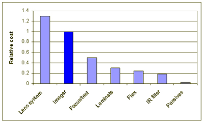
Sensor Packaging for Camera-Phone Module by Tessera
Video/Imaging Design Line: Tessera's Giles Humpston and Michael Nystrom discuss the trade-offs in camera module design. Although the article is obviously biased towards Sellcase packaging, it gives a good overview of sensor packaging techniques for camera-phone module.
A relative costs chart for 1.3MP camera-phone module components from the article:
Article has an interesting claim concerning image sensor wafer thickness:
For conventional semiconductors, the industry is moving toward ever thinner die. Wafers are now routinely thinned to 75µm thickness, and even 25µm is being practiced in high-volume manufacture. The underlying advances in wafer thinning technology have enabled some of the remarkably slim format products and electronics accessories that are now available. Notable examples are flash memory cards, smart credit cards and the complexity of functionality that can now be crammed into USB devices.
By comparison, CMOS image sensors appear to be stuck in the Dark Ages with die thicknesses of hundreds of microns. There are two good reasons for this. The first is that the depth of black color (i.e. absence of light) that an imager is able to detect is determined by the leakage current of the photodiodes and certain active devices in the imaging array. This property is known as the "dark current" and can be measured. As a general rule, the dark current will increase as the semiconductor wafer thickness diminishes, and hence this metric affects the low light performance of the camera.
The second consideration is mechanical. When the glass cover is attached to the imager, the center region of the die is provided with mechanical reinforcement. This leaves vulnerable protruding ledges where the bond pads are located. If the die is too thin, the fragility of these ledges is reflected in manufacturing yield loss.
Thursday, December 14, 2006
Tessera Introduces a New Thinner Wafer-Level Chip-Size Packaging
Advanced Imaging Pro: Tessera Technologies announced SHELLCASE(R) RT, one of the world's thinnest, wafer-level chip size packaging (WLCSP). As one of the thinnest WLCSPs on the market today (at ~500microns), SHELLCASE(R) RT enables very low profile camera modules.
Forza Silicon and IBM to Collaborate
Yahoo: Forza Silicon and IBM announced that they are collaborating to develop CMOS image sensor chips using IBM's CMOS Image Sensor Foundry (CIMG) process, and characterizing IBM's image sensor IP. IBM's CIMG foundry, based in Essex Junction, VT, uses 180-nm and 130-nm copper process technology with 4T image sensor IP. Forza contributes mixed signal IC design services and products to IBM Technology Foundry program.
Wednesday, December 13, 2006
New iSuppli Market Data
Digitimes: Mobile phones have emerged as the single largest market for image sensors, surpassing the entire consumer electronics segment to become the main application for both charge-coupled device (CCD) and CMOS image sensors, according to iSuppli.
Revenue from shipments of image sensors for mobile phones will grow to US$5.9 billion by 2010, increasing at a compound annual growth rate (CAGR) of 27.4%, up from US$1.7 billion in 2005. Unit shipments of image sensors to mobile phones will grow to 1.2 billion by 2010, increasing at a CAGR of 19.7%, up from 484 million units in 2005.
In 2005, 199 million image sensors were sold for all other applications outside of mobile phones, including digital still cameras. By 2010, this disparity will grow more, with nearly 1.2 billion sensors shipped for mobile handsets and slightly less than 350 million shipped for other applications.
Although cameras have become standard on most mobile phones, studies suggest that actual usage remains much lower, with less than 10% of consumers actually using the device as their primary image capture device. Digital still cameras remain the device of choice for capturing images digitally mainly because of the lower image quality in mobile handsets, drawbacks in form factors and ease of operation in mobile phones and difficulties and sometimes the cost of transferring photos from a user's phone to another device, such as a PC.
These challenges are exacerbated by two other factors: marketing from digital still camera manufacturers and user experiences.
In the first case, camera makers have successfully trained consumers into thinking they need more megapixels than they actually require.
The second factor is the difficulties users face with phone cameras when trying to perform common photography tasks like printing, cropping and zooming. Cameras generally need between four and five megapixels to support these tasks. However, users may have to get accustomed to low-resolution camera phone pictures because at the current rate of advancement, the average camera phone will not reach the four to five megapixel level range until 2010.
ProMOS Expands into Image Sensors
Digitimes: At its 10th anniversary celebration, DRAM maker ProMOS Technologies reaffirmed the company's expansion plans including entering CMOS image sensor production.
Tuesday, December 12, 2006
Micron expands Bracknell design center
EETimes: Micron plans to add another 30 engineers to bring the Bracknell design center total up to 90 by the middle of next year.
Asked whether the mix of talents required at Bracknell had altered following the acquisition of Avago's image sensor business, David Burrows, director of the centre, said: "Not at all. The Avago groups will continue to focus on mainstream products, for example chips, sensors and SoCs. We will do that here as well, but also build up our portfolio of IP libraries and building blocks that will be used by designers throughout the image sensors group."
Burrows added that the Avago acquisition did not include any manufacturing capacity, since Micron has sufficient production capability for CMOS image sensors at its wafer fabs in Boise and Avezzano, Italy.
Many of the center's new recruits came from Agere, which closed a design group just a few miles away.
Micron Acquires Avago's Image Sensor Business
Yahoo-Finance: Micron acquires Avago Technologies' image sensor business for approximately $53M, plus contingent payments payable to Avago if certain milestones are met.
The acquisition provides Micron with an experienced imaging team, select imaging products and intellectual property relating to Avago's image sensor business. The Avago imaging team joining Micron consists of about 90 employees, mostly engineers, from Corvallis, Ore.; Fort Collins, Colo.; San Jose, Calif.; and Penang, Malaysia.
It's not immediately clear if optical mouse sensors are included in the deal.
Friday, December 08, 2006
More about Canesta
EETimes put a description of Canesta 3D sensing technology together with few more bits of interesting information:
Canesta outsources its manufacturing to Tower Semiconductor. Its 3-D CMOS image sensors are cast in a 180-nanometer process. Its business model calls for it to sell camera modules to OEMs and to license its technology to manufacturers that want to make their own cameras able to perceive in 3-D. So far it has sold about 100 development kits to OEMs and manufacturers for apps as varied as video games, industrial automation and automobiles.
Honda Motor Co. Ltd. has made investments in Canesta totaling more than $5 million over three years.
Thursday, December 07, 2006
Digicam Market Research
Solid State Technology: After five years of double-digit growth, the digital camera market is leveling off to a plateau of roughly $18 billion/year as most users have already converted from film photography. The next big growth trend to watch -- the crossover for CMOS image sensors to surpass charge-coupled devices (CCD), according to data from IC Insights Inc.
After quadrupling in value from 2001-2004, the digital still camera market is expected to slow down to just 5% growth in 2006 to $18.1 billion, and remain basically flat through the end of the decade, while unit shipments ratchet down from a 38% compound annual growth rate (CAGR) from 2000-2005 to just 6% CAGR from 2006-2010. About 81.9 million standalone digital cameras are expected to be sold in 2007, a 7% increase from 2006.
An important trend in digital cameras is growing adoption of high-speed CMOS image sensors, which are already in most embedded cell-phone cameras, but now increasingly used in "hybrid" models offering both high-resolution still pictures as well as high-definition full-motion videos. About 79% of today's digital still cameras still use CCDs, but IC Insights projects a crossover by 2009 where CMOS image sensors surpass CCDs in digital still cameras.
This year, Micron has surpassed fabless OmniVision as the top image sensor supplier, with sales surging 147% in its just-closed fiscal 2006 (through August) to $749 million, about 14% of its overall revenues, a 7.5xfold increase from 2004's $99 million. The company is utilizing old DRAM fab lines in the US, Italy, and Japan to produce CMOS image sensors, including a closed 200mm fab in Idaho purchased from Zilog restarted for image sensor work.
Most of the top CCD makers are in Japan (e.g., Matsushita, Fujifilm Microdevices), although Kodak has a CCD fab in New York. But several CCD makers including Sony, Sharp and Toshiba are shifting capacity to CMOS image sensors, and even Samsung is expanding its output of CMOS image sensors.
TSMC Acquires XinTec Shares
Digitimes: TSMC announced that it has acquired 90.5 million shares of XinTec, an IC packaging house specializing in CCD and CMOS image sensor wafer-level packaging, through a private placement with the total investment being NT$1.357 billion (US$42 million).
After the investment, TSMC has a 43% stake in XinTec.
Wednesday, December 06, 2006
Canesta High DR Patent Granted
Yahoo-Finance: The new Canesta SunShield(TM) technology has been granted U.S. Patent No. 6,919,549, "Method and System to Differentially Enhance Sensor Dynamic Range."
A key challenge in uncontrolled lighting conditions, such as those common in automotive applications, has been dealing with both bright sunlight and the rapidly flickering shadows that often accompanies it. Canesta's native technology uses bursts of infrared light from tiny lasers or light-emitting diodes (LEDs) to illuminate the field of view, and then measures the "time of flight" that it takes the photons of infrared light to bounce off of nearby objects and return to the sensor. From this, the sensor chips form a real-time 3-dimensional image, at 30 frames per second or better, which can be used to detect objects.
In the presence of strong sunlight, however, the extremely low-level illumination from the laser or LED is, in effect, swamped out. If a system is made sensitive enough to perceive the infrared bursts, then it completely saturates in the presence of bright light, not unlike our eyes do when surprised by a camera flash. By contrast, if the system is configured to work at the highest levels of sunlight, then the infrared pulses become too faint to measure accurately.
Canesta solved this problem with a simple and elegant solution. Rather than allowing the sensor to saturate by having it observe the scene for too long a time - in this case the duration of one "frame," a series of shorter samples are taken that keeps the amount of ambient light for any one sample within the dynamic range of the sensor. During each sample, the system receives photons from both the ambient background and from the infrared ranging signals. At the end of the sample, the signal from the ambient sources is simply discarded, while the ranging signal is saved. When the time comes for the sensor array to output a frame - say, every 30th of a second - the results from each sample, which now only contain the ranging signal component, are added together to determine its final value.
Tuesday, December 05, 2006
Image Sensor Pricing
Global Sources published the image sensors pricing info on Chinese market: Currently (Sept 26, 2006), 2MP CMOS sensors are quoted between $4.5 and $5. Taiwan makers expect prices to decrease by 10 percent to 20 percent throughout the rest of the year due to stiff competition and supply surge.
CIF and VGA CMOS image sensors are offered at about $1 per unit.
1.3MP CMOS image sensors are quoted at $2 to $3.50, while 2MP CMOS sensors come at $4 to $5 per unit (a slight contradiction with the numbers above). Quotes for 3MP CMOS image sensors range between $6.50 and $8.
An other part of the article gives some global image sensor market data:
The global market for image sensors continues on an upward trend, with total revenues expected to rise from $3.86 billion last year to $4.44 billion this year, according to research firm In-Stat/MDR. The CMOS image sensor market continues to expand due to the popularity of camera phones and digital still cameras (DSCs) as primary applications, and PC cameras, toys and optical mice as secondary applications. The segment estimates total revenues of $2 billion this year, up from $1.4 billion in 2005. Likewise, the emerging market for contact image sensors (CIS) estimates revenues of $409 million this year, up from $340 million.
On the other hand, the CCD image sensors market will experience a gradual decline in revenues from $2.1 billion last year to $2 billion this year. The segment estimates total revenues of $1.3 billion by 2009, accounting for less than 30 percent of the market.
Saturday, December 02, 2006
3D Imagers in Automotive and Mashine Vision Apps
EETimes: The automotive sensor market already tops $2.5 billion, according to ABI Research (Oyster Bay, N.Y.). Another $750 million is divided among security, industrial automation and videogaming uses of electronic sensors, according to Frost & Sullivan, the Automated Imaging Association and Piper Jaffray, respectively.
Said this, the article concentrates on Canesta 3D Imager and its applications in automotive.
Notebook Imager Requirements and Trade-Offs
Shone Tran from Cypress published an article in Video/Imaging Design Line on image sensor design for notebook webcams. Obviously, the article is biased toward Cypress products, but gives a good review of webcam requirements anyway.
Friday, December 01, 2006
Rice University 1-pixel Imager
Electronic Design mentions Rice University 1-pixel imager in an undated article:
This controversial idea was presented a few months ago and was widely debated then. Most opinions are that the light sensitivity of this sensor is very low, so its applications are limited.
Taiwan and Korea CIS Update
Global Sources published an aritcle on Far Eastern CIS manufacturers news. The most interesting product to come is from Pixart. PixArt Technologies Inc. from Taiwan plans to develop integrated image sensors and low power optical mouse sensors for wireless applications this year.
Pixart also plans to develop 4T pixel color/mono image sensors - quite a lete decision in the time where the whole industry is 4T already.
Silicon Optronics Inc. (SOI) plans to release 3MP image sensors in the near future. At present, its product line includes 2.1MP UXGA, 1.3MP SXGA and VGA color image sensors. Models from the VGA series such as the SOI763A with 1/4in lens size are among its bestsellers.
LiteOn Semiconductor Corp. offers contact-type monochrome CIS and color CIS. LiteOn's product roadmap for the year includes low noise 3.3V/600dpi color CIS, low-cost 3.3V/1,200dpi color CIS, ultra fast three-channel 3.3V/1,200dpi color CIS, linear fingerprint image sensors for mobile phones, and laser mouse image sensors.
SiliconFile Technologies Inc. recently introduced a 1.3MP model, the NOON130PC20, which incorporates a 1,308x1-52 pixel array, on-chip 10bit ADC, and an image signal processor. It has 1/3.8in optical format and supports 15fps (SXGA), and 30fps (VGA) frame rate. Its sensor technology enhances image quality by reducing FPN, horizontal and vertical line noise and random noise, and supports 15fps (UXGA) and 30fps (SVGA) frame rate.
Pixelplus Co. Ltd, plans to release by year-end its PO5130 1.3MP CMOS image sensor that integrates an array of 1,280x1,024 effective SXGA resolution. The device uses 0.13µm process technology with improved image quality under low light conditions.
For camera phone applications, VGA image sensors dominated the market last year. Makers expect 1.3MP models to finally surpass VGA this year. Makers believe that higher resolution image sensors including 3MP and 5MP models used in 2.5G or 3G camera phones will not become the market standard until 2008.