Lists

Tuesday, October 31, 2023

Metalenz announces polarization sensor for face ID

Press release: https://metalenz.com/metalenz-launches-polar-id-enabling-simple-secure-face-unlock-for-smartphones/

Metalenz Launches Polar ID, Enabling Simple, Secure Face Unlock for Smartphones 

  • The world’s first polarization sensor for smartphones, Polar ID provides ultra-secure facial authentication in a condensed footprint, lowering implementation cost and complexity.
  •  Now demonstrated on Qualcomm Technologies’ latest Snapdragon mobile platform, Polar ID is poised to drive large-scale adoption of secure face unlock across the Android ecosystem.

Boston, MA – October 26, 2023 Meta-optics industry leader Metalenz unveiled Polar ID, a revolutionary new face unlock solution, at Qualcomm Technologies’ annual Snapdragon Summit this week. Being the world’s only consumer-grade imaging system that can sense the full polarization state of light, Polar ID enables the next level of biometric security. Using breakthrough advances in meta-optic capability, Polar ID accurately captures the unique “polarization signature” of a human face. With this additional layer of information, even the most sophisticated 3D masks and spoof instruments are immediately detected as non-human.


Facial authentication provides a seamless method for unlocking phones and allowing digital payment. However, to make the solution sufficiently secure requires expensive, bulky, and often power-hungry optical modules. Historically, this has limited the implementation of face unlock to only a few high-end phone models. Polar ID harnesses meta-optic technology to extract additional information such as facial contour details and to detect human tissue liveness from a single image. It is significantly more compact and cost effective than incumbent “Structured Light” face authentication solutions which require an expensive dot-pattern projector and multiple images.


Now demonstrated on a smartphone reference design powered by the new Snapdragon® 8 Gen 3 Mobile Platform, Polar ID has the efficiency, footprint, and price point to enable any Android smartphone OEM to bring the convenience and security of face unlock to the 100s of millions of mobile devices that currently use fingerprint sensors.

“Size, cost, and performance, those are the key metrics in the consumer industry”, said Rob Devlin, Metalenz CEO & Co-founder. “Polar ID offers an advantage in all three. Its small enough to fit in the most challenging form factors, eliminating the need for a large notch in the display. Its secure enough that it doesn’t get fooled by the most sophisticated 3D masks. Its substantially higher resolution than existing facial authentication solutions, so even if you’re wearing sunglasses and a surgical mask, the system still works. As a result, Polar ID delivers secure facial recognition at less than half the size and cost of incumbent solutions.”


“With each new generation of our flagship Snapdragon 8 series, our goal is to deliver the next generation of cutting-edge smartphone imaging capabilities to consumers. Our advanced Qualcomm® Spectra™ ISP and Qualcomm® Hexagon™ NPU were specifically designed to enable complex new imaging solutions, and we are excited to work with Metalenz to support their new Polar ID biometric imaging solution on our Snapdragon mobile platform for the first time,” said Judd Heape, VP of Product Management, Qualcomm Technologies, Inc.


“Polar ID is a uniquely powerful biometric imaging solution that combines our polarization image sensor with post-processing algorithms and sophisticated machine learning models to reliably and securely recognize and authenticate the phone’s registered user. Working closely with Qualcomm Technologies to implement our solution on their reference smartphone powered by Snapdragon 8 Gen 3, we were able to leverage the advanced image signal processing capabilities of the Qualcomm Spectra ISP while also implementing mission critical aspects of our algorithms in the secure framework of the Qualcomm Hexagon NPU, to ensure that the solution is not only spoof-proof but also essentially unhackable” said Pawel Latawiec, CTO of Metalenz. “The result is an extremely fast and compute efficient face unlock solution ready for OEMs to use in their next generation of Snapdragon 8 Gen 3-powered flagship Android smartphones.”


Polar ID is under early evaluation with several top smartphone OEMs, and additional evaluation kits will be made available in early 2024. Metalenz will exhibit its revolutionary Polar ID solution at MWC Barcelona and is now booking meetings to showcase a live demo of the technology to mobile OEMs.
Contact sales@metalenz.com to reserve your demo.


Monday, October 30, 2023

Fraunhofer IMS 10th CMOS Imaging Workshop Nov 21-22 in Duisburg, Germany

https://www.ims.fraunhofer.de/en/Newsroom/Fairs-and-events/10th-cmos-imaging-workshop.html

10th CMOS Imaging Workshop 

What to expect
You are kindly invited to an exciting event, which will promote the exchange of users, developers and researchers of optical sensing to enhance synergy and pave the way to great applications and ideas.

Main topics

  •  Single photon imaging
  •  Spectroscopy, scientific and medical imaging
  •  Quantum imaging
  •  Image sensor technologies

The workshop will not be limited to CMOS as a sensor technology, but will be fundamentally open to applications, technologies and methods based on advanced optical sensing.


Job Postings - Week of 29 Oct 2023


PRADCO Outdoor Brands

Electrical Engineer

Birmingham, Alabama, USA

Link

Karl Storz

Electronics Component Engr IV

Goleta, California, USA

Link

Omnivision

Staff Process Integration Engineer

 Santa Clara, California, USA

Link

Oxford Instruments - Andor

Senior Electronic Engineer

Belfast, Northern Ireland, UK

Link

Chromasens

Senior Project Manager Image Processing Systems / Machine Vision

Konstanz, Germany

Link

Teledyne e2v

Technical Product Manager

Chelmsford, England, UK

Link

ETH Zurich

 PhD Position in Imaging Sensor Optimization, Control and Image Reconstruction

Zurich, Switzerland

Link


Jobs from earlier lists

Posting links will remain here for six months but many of them will have expired.

2024

18 Aug - 21 Jul - 16-Jun - 2-Jun -19-May - 5-May - 21-Apr - 14-Apr - 7-Apr

Sunday, October 29, 2023

Conference List - March 2024

5th workshop on Image Sensors for Precision Astronomy (ISPA) - 12-14 March 2024 - Menlo Park, California, USA - Website

20th Annual Device Packaging Conference - 18-21 Mar 2024 - Scottsdale, Arizona, USA - Website

Image Sensors Europe - 20-21 Mar 2024 - London, UK - Website

Laser World of Photonics China - 20-22 Mar 2024 - Shanghai, China - Website


Return to Conference List Index  

Friday, October 27, 2023

Prophesee announces GenX320 low power event sensor for IoT applications

Press release: https://prophesee-1.reportablenews.com/pr/prophesee-launches-the-world-s-smallest-and-most-power-efficient-event-based-vision-sensor-bringing-more-intelligence-privacy-and-safety-than-ever-to-consumer-edge-ai-devices

Prophesee launches the world’s smallest and most power-efficient event-based vision sensor, bringing more intelligence, privacy and safety than ever to consumer Edge-AI devices

Prophesee’s latest event-based Metavision® sensor - GenX320 - delivers new levels of performance including ultra-low power, low latency, high flexibility for efficient integration in AR/VR, wearables, security and monitoring systems, touch-free interfaces, always-on IoT and many more

October 16, 2023 2pm CET PARIS –– Prophesee SA, inventor of the world’s most advanced neuromorphic vision systems, today announced the availability of the GenX320 Event-based Metavision sensor, the industry’s first event-based vision sensor developed specifically for integration into ultra-low-power Edge AI vision devices. The fifth generation Metavision sensor, available in a tiny 3x4mm die size, expands the reach of the company’s pioneering technology platform into a vast range of fast-growing intelligent Edge market segments, including AR/VR headsets, security and monitoring/detection systems, touchless displays, eye tracking features, always-on smart IoT devices and many more.

The GenX320 event-based vision sensor builds on Prophesee’s track record of proven success and expertise in delivering the speed, low latency, dynamic range and power efficiency and privacy benefits of event-based vision to a diverse array of applications.

The 320x320 6.3μm pixel BSI stacked event-based vision sensor offers a tiny 1/5” optical format. It has been developed with a specific focus on the unique requirements of efficient integration of innovative event sensing in energy-, compute- and size-constrained embedded at-the-edge vision systems. The GenX320 enables robust, high-speed vision at ultra-low power and in challenging operating and lighting conditions.

GenX320 benefits include:

  •  Low latency µsec resolution timestamping of events with flexible data formatting.
  •  On-chip intelligent power management modes reduce power consumption to as low as 36uW and enable smart wake-on-events. Deep sleep and standby modes are also featured.
  •  Easy integrability/interfacing with standard SoCs with multiple integrated event data pre-processing, filtering, and formatting functions to minimize external processing overhead.
  •  MIPI or CPI data output interfaces offer low-latency connectivity to embedded processing platforms, including low-power microcontrollers and modern neuromorphic processor architectures.
  •  AI-ready: on-chip histogram output compatible with multiple AI accelerators;
  •  Sensor-level privacy-enabled thanks to event sensor’s inherent sparse frameless event data with inherent static scene removal.
  •  Native compatibility with Prophesee Metavision Intelligence, the most comprehensive, free, event-based vision software suite, used by a fast-growing community of 10,000+ users.

“The low-power Edge-AI market offers a diverse range of applications where the power efficiency and performance characteristics of event sensors are ideally suited. We have built on our foundation of commercial success in other application areas and developed this new event-based Metavision sensor to address the needs of Edge system developers with a sensor that is easy to integrate, configure and optimize for multiple compelling use cases in motion and object detection, presence awareness, gesture recognition, eye tracking, and other high growth areas,” said Luca Verre, CEO and co-founder of Prophesee.


Specific use case potential

  •  High speed eye-tracking for foveated rendering for seamless interaction in AR/VR/XR headsets
  •  Low latency touch-free human machine interface in consumer devices (TVs, laptops, game consoles, smart home appliances and devices, smart displays and more)
  •  Smart presence detection and people counting in IoT cameras and other devices
  •  Ultra-low power always-on area monitoring systems
  •  Fall detection cameras in homes and health facilities

Availability
The GenX320 is available for purchase from Prophesee and its sales partners. It is supported by a complete range of development tools for easy exploration and optimization, including a comprehensive Evaluation Kit housing a chip on board (COB) GenX320 module, or a compact optical flex module. In addition, Prophesee is offering a range of adapter kits that enable seamless connectivity to a large range of embedded platforms, such as a STM32 MCU, enabling faster time-to-market.


Early adopters
Zinn Labs
“Zinn Labs is developing the next generation of gaze tracking systems built on the unique capabilities of Prophesee’s Metavision event sensors. The new GenX320 sensor meets the demands of eye and gaze movements that change on millisecond timescales. Unlike traditional video-based gaze tracking pipelines, Zinn Labs is able to leverage the GenX320 sensor to track features of the eye with a fraction of the power and compute required for full-blown computer vision algorithms, bringing the footprint of the gaze tracking system below 20 mW. The small package size of the new sensor makes this the first time an event-based vision sensor can be applied to space-constrained head-mounted applications in AR/VR products. Zinn Labs is happy to be working with Prophesee and the GenX320 sensor as we move towards integrating this new sensor into upcoming customer projects.”
Kevin Boyle, CEO & Founder
 

XPERI
“Privacy continues to be one of the biggest consumer concerns when vision-based technology is used in our products such as DMS and TV services. Prophesee’s event-based Metavision technology enables us to take our ‘privacy by design’ principle to an even more secure level by allowing scene understanding without the need to have explicit visual representation of the scene. By capturing only changes in every pixel, rather than the entire scene as with traditional frame-based imaging sensors, our algorithms can derive knowledge to sense what is in the scene, without a detailed representation of it. We have developed a proof-of-concept demo that demonstrates DMS is fully possible using neuromorphic sensors. Using a 1MP neuromorphic sensor we can infer similar performance as an active NIR illumination 2MP vision sensor-based solution. Going forward, we focus on the GenX320 neuromorphic sensor that can be used in privacy sensitive smart devices to improve user experience.”
Petronel Bigioi, Chief Technology Officer
 

ULTRALEAP
“We have seen the benefits of Prophesee’s event-based sensors in enabling hands-free interaction via highly accurate gesture recognition and hand tracking capabilities in Ultraleap’s TouchFree application. Their ability to operate in challenging environmental conditions, at very efficient power levels, and with low system latency enhances the overall user experience and intuitiveness of our touch free UIs. With the new Genx320 sensor, these benefits of robustness, low power consumption, latency and high dynamic range can be extended to more types of applications and devices, including battery-operated and small form factors systems, proliferating hands-free use cases for increased convenience and ease of use in interacting with all sorts of digital content.”
Tom Carter, CEO & Co-founder

Additional coverage on EETimes:

https://www.eetimes.com/prophesee-reinvents-dvs-camera-for-aiot-applications/

Prophesee’s GenX30 chip, sensor die at the top, processor at the bottom. ESP refers to the digital event signal processing pipeline. (Source: Prophesee)


Thursday, October 26, 2023

Omnivision's new sensor for security cameras

OMNIVISION Announces New 4K2K Resolution Image Sensor for Home and Professional Security Cameras
 
The OS08C10 is a high-performance 8MP resolution, small-form-factor image sensor with on-chip staggered and DAG HDR technology, designed to produce superb video/image quality in challenging lighting environments
 
SANTA CLARA, Calif. – October 24, 2023 – OMNIVISION, a leading global developer of semiconductor solutions, including advanced digital imaging, analog, and touch & display technology, today announced the new OS08C10, an 8-megapixel (MP) backside illumination (BSI) image sensor that features both staggered high dynamic range (HDR) and single exposure dual analog gain (DAG) for high-performance imaging in challenging lighting conditions. The 1.45-micron (µm) BSI pixel supports 4K2K resolution and high frame rates. It comes in a small 1/2.8-inch optical format, a popular size for home and professional security, IoT and action cameras.
 
“Our new 1.45 µm pixel OS08C10 image sensor provides improved sensitivity and optimized readout noise, closing the gap with big-pixel image sensors that have traditionally been required for high-performance imaging in the security market,” said Cheney Zhang, senior marketing manager, OMNIVISION. “The OS08C10 supports both staggered HDR and DAG HDR. Staggered HDR extends dynamic range in both bright and low lighting conditions; the addition of built-in DAG provides single-exposure HDR support and reduces motion artifacts. Our new feature-packed sensor supports 4K2K resolution for superior image quality with finer details and enhanced clarity.”
 
OMNIVISION’s OS08C10 captures real-time 4K video at 60 frames per second (fps) with minimal artifacts. Its selective conversion gain (SCG) pixel design allows the sensor to flexibly select low and high conversion gain, depending on the lighting conditions. The sensor adopts the new correlated multi-sampling (CMS) to further reduce readout noise and improve SNR1 and low-light performance. The OS08C10’s on-chip defective pixel correction (DPC) improves quality and reliability above and beyond standard devices by providing real-time correction of defective pixels that can result throughout the sensor’s life cycle, especially in harsh operating conditions.
 
The OS08C10 is built on OMNIVISION’s PureCel®Plus-S stacked-die technology, enabling high-resolution 8MP in a small 1.45 µm BSI pixel. At 300 mW (60 fps), the OS08C10 achieves the lowest power consumption on the market. OMNIVISION’s OS08C10 is a cost-effective 4K2K solution for security, IoT and action cameras applications.
 
The OS08C10 is sampling now and will be in mass production in Q1 2024. For more information, contact your OMNIVISION sales representative: www.ovt.com/contact-sales.


Wednesday, October 25, 2023

Sony introduces IMX900 stacked CIS

Sony Semiconductor Solutions to Launch 1/3-Type-Lens-Compatible, 3.2-Effective-Megapixel Stacked CMOS Image Sensor with Global Shutter for Industrial Use Featuring Highest Resolution in This Class in the Industry

Atsugi, Japan — Sony Semiconductor Solutions Corporation (SSS) today announced the upcoming release of the IMX900, a 1/3-type-lens-compatible, 3.2-effective-megapixel stacked CMOS image sensor with a global shutter for industrial use that boasts the highest resolution in its class.
The new sensor product employs an original pixel structure to dramatically improve light condensing efficiency and near infrared sensitivity compared to conventional products, enabling miniaturization of pixels while maintaining the key characteristics required of industrial image sensors. This design achieves the industry’s highest resolution of 3.2 effective megapixels for a 1/3.1-type, global shutter system which fits in the S-mount (M12), the mount widely used in compact industrial cameras and built-in vision cameras.

The new product will contribute to the streamlining of industrial tasks in numerous ways, by serving in applications such as code reading in the logistics market and assisting in automating manufacturing processes using picking robot applications on production lines, thereby helping to resolve issues in industrial applications.

With demand for automation and manpower savings on the rise in every industry, SSS’s original Pregius S™ global shutter technology contributes to improved image recognition by enabling high-speed, high-precision, motion distortion-free imaging in a compact design. The new sensor utilizes a unique pixel structure developed based on Pregius S, moving the memory unit that was previously located on the same substrate as the photodiode to a separate signal processing circuit area. This new design makes it possible to enlarge the photodiode area, enabling pixel miniaturization (2.25 μm) while maintaining a high saturation signal volume, successfully delivering a higher pixel count of approximately 3.2 effective megapixels for a 1/3.1-type sensor.

Moving the memory unit to the signal processing circuit area has also increased the aperture ratio, bringing significant improvements to both incident light angle dependency and quantum efficiency. These features enable a much greater level of flexibility in the lens design for the cameras which employ this sensor. Additionally, a thicker photodiode area enhances the near infrared wavelength (850 nm) sensitivity, and nearly doubles the quantum efficiency compared to conventional products.

This compact, 1/3.1-type product is available in a package size that fits in the S-mount (M12), the versatile mount type used in industrial applications. It can be used in a wide range of applications where more compact, higher performance product designs are desired, such as in compact cameras for barcode readers in the logistics market, picking robot cameras on production lines, and the automated guided vehicles (AGVs) and autonomous mobile robots (AMRs) that handle transportation tasks for workers.

Main Features

  •  Industry’s highest resolution for an image sensor with a global shutter compatible with a 1/3-type lens, at approximately 3.2 effective megapixels
  •  Vastly improved incident light angle dependency lend greater flexibility to lens design
  • Delivers approximately double the quantum performance of conventional products in the near infrared wavelength
  • Includes on-chip features for greater convenience in reducing post-production image processing load
  • High-speed, 113 fps imaging


Cross-section of pixel structure
Product using conventional Pregius S technology (left) and the IMX900 using the new pixel structure (right)

Example of effects due to improved incident light angle dependency

Imaging comparison using near-infrared lighting (850 nm)
(Comparison in 2.25 μm pixel equivalent using conventional Pregius structure)


Usage example of Fast Auto Exposure function


Monday, October 23, 2023

Gpixel introduces 5MP and 12MP MIPI-enabled CIS

Gpixel adds MIPI-enabled 5 MP and 12 MP NIR Global Shutter image sensors to popular GMAX family


October 18, 2023, Changchun, China: Gpixel announces the pin-compatible GMAX3405 and
GMAX3412 CMOS image sensors - both based on a high-performance 3.4 μm charge domain global
shutter pixel to complete its c-mount range of GMAX products. With options for read out via either
LVDS or MIPI channels, these new sensors are optimized for easy integration into cost-sensitive
applications in machine vision, industrial bar code reading, logistics, and traffic.


GMAX3405 provides a 2448(H) x 2048(V), 5 MP resolution in a 2/3” optical format. In 10-bit mode,
reading out through all 12 pairs of LVDS channels, the frame rate is over 164 fps. In 12-bit mode,
100 fps can be achieved. Using the 4 MIPI D-PHY channels, the maximum frame rate is 73 fps with
a 12-bit depth. GMAX3412 provides a 4096(H) x 3072(V), 12 MP resolution in a 1.1” optical format.
In 10-bit mode, reading out through all 16 pairs of LVDS channels, the frame rate is over 128 fps.
In 12-bit mode, 60 fps can be achieved. Using the 4 MIPI D-PHY channels, the maximum frame rate
is 30 fps with a 12-bit depth. In both sensors, various multiplexing options are available for both
LVDS and MIPI readout to reduce the number of lanes.

 The 3.4 μm charge-domain global shutter pixel achieves a full well capacity of 10 ke- and noise of
3.6 e- at default x1 PGA gain, down to 1.5 e- at max gain setting (x16), delivering up to 68.8 dB
linear dynamic range. The advanced pixel design and Red Fox technology combined brings a peak
QE of 75% @ 540 nm, a NIR QE of 33% @850 nm , a Parasitic Light Sensitivity of -88 dB and an
excellent angular response of > 15° @ 80% response. All of this combined with multislope HDR
mode and ultra-short exposure time modes down to 1 us.


“The GMAX family was originally known for the world’s first 2.5 μm global shutter pixel. As the
product family grows, we are leveraging the advanced technology that makes the 2.5 μm pixel
possible to bring more generous light sensitivity with larger pixel sizes fitting mainstream optical
formats. With the addition of the MIPI interface and pin-compatibility and excellent NIR response,
these 2 new models bring more flexibility and cost-effectiveness to the GMAX product family.” says
Wim Wuyts, Gpixel’s Chief Commercial Officer.


Both GMAX3405 and GMAX3412 are housed in 176 pin ceramic LGA packages, both being pin-
compatible to each other. The outer dimensions of the 5MP and 12MP sensors respectively are
17.60 mm x 15.80 mm and 22.93 mm x 19.39 mm. The LGA pad pattern is optimized for reliable
solder connections and the sensor assembly includes a double-sided AR coated cover glass lid.

Engineering samples of both products, in both color and monochrome variants, can be ordered
today for delivery in November 2023. For more information about Gpixel’s roadmap of products
for industrial imaging, please contact info@gpixel.com to arrange for an overview.

Job Postings - Week of 22 Oct 2023

 A few interesting samples:

Onsemi

Principal Product Engineer

Meridian, Idaho, USA

Link

Sony

Image Sensor Device/Pixel Research & Development

Atsugi, Japan

Link

Quantum-Si

Engineering Technician

Branford, Connecticut, USA

Link

Allied Vision

Test Manager - Camera Development

Ahrensburg, Osnabrück, Germany

Link

Lockheed-Martin

Electro-Optical Engineer - Early Career

Orlando, Florida, USA

Link

Olympus

Global VP R&D - Single-Use Endoscopy

Southborough, Massachusetts, USA

Link

MIT

Postdoctoral Associate, Computational Imaging

Cambridge, Massachusetts, USA

Link

IMEC

Internship & Thesis - Metasurface color splitters for highly efficient image sensors

Leuven, Belgium

Link


Sunday, October 22, 2023

Reticon-PerkinElmer-Excelitas Documentation

This entry covers the progression of products originally developed by Reticon through its acquisition by EG&G (retaining the Reticon name) then EG&G's acquisition of part of PerkinElmer and the PerkinElmer name (Reticon was still applied sporadically as a brand) and finally the spinoff of PerkinElmer's optoelectronics businesses as Excelitas. Throughout this process, many of the original Reticon products retained their original part numbers as can be seen in the data sheets. 

Four items of note:

1 - Documents issued under "EG&G Reticon" are in the Reticon folder since the Reticon identity was maintained.  There is not yet an EG&G folder but this will be added when the amorphous silicon flat-panel products developed by EG&G are covered. The EG&G Amorphous Silicon facility was in the same building as Reticon in Sunnyvale, California, but operated independently. That business was later sold by PerkinElmer to Varex, formerly Varian Medical Systems.

2 - Excelitas no longer sells any Reticon-originated products. These became difficult to source when the fab Reticon operated in its own building was closed in the late 90's. Moving from a 3 micron process to 180 nm was quite difficult, especially while the selection of fabs who could make CCDs was rapidly shrinking. Excelitas still sells products originally made by some of the other optoelectronics companies EG&G bought, like thermopile arrays.  Those are included in the Excelitas folder but their history will be told later.

3 - Reticon, up through the PerkinElmer days, made many custom devices including a 20,000 pixel long three-color TDI sensor that flew on the U2 and an ultraviolet CCD for i-line semiconductor mask inspection. If the specifications or evaluation reports for any of these turn up, they will be posted.

4 - Reticon started by making bucket-brigade devices to be used as delay lines and switched-capacitor filter chips. These aren't imagers but they are in the folder to provide some background.

Reticon & EG&G Reticon document archive

PerkinElmer document archive

Excelitas document archive

Return to the Documentation List

Wednesday, October 18, 2023

Galaxycore announces dual analog gain HDR CIS

Press release: https://en.gcoreinc.com/news/detail-66

GalaxyCore Unveils Industry's First DAG Single-Frame HDR 13Megapixels CIS

2023.08.11

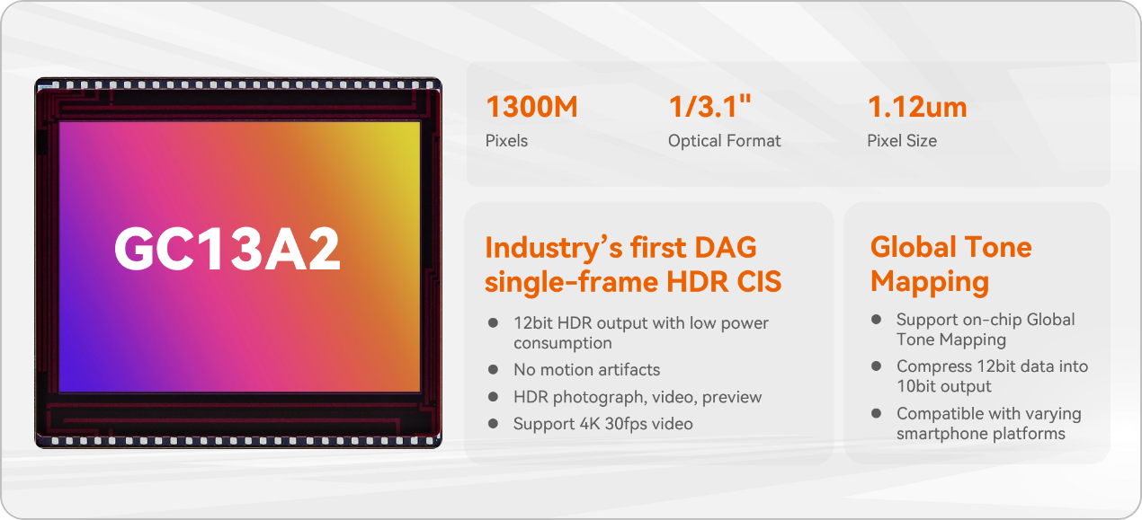
GalaxyCore has officially launched the industry's first 13megapixels image sensor with Single-Frame High Dynamic Range (HDR) capability – the GC13A2. This groundbreaking 1/3.1", 1.12μm pixel back-illuminated CIS features GalaxyCore's unique Dual Analog Gain (DAG) circuit architecture, enabling low-power consumption 12bit HDR output during previewing, photography, and video recording. This technology enhances imaging dynamic range for smartphones, tablets, and more, resulting in vividly clear images for users.

The GC13A2 also supports on-chip Global Tone Mapping, which compresses real-time 12bit data into 10bit output, preserving HDR effects and expanding compatibility with a wider range of smartphone platforms.


High Dynamic Range Technology

Dynamic range refers to the range between the darkest and brightest images an image sensor can capture. Traditional image sensors have limitations in dynamic range, often failing to capture scenes as perceived by the human eye. High Dynamic Range (HDR) technology emerged as a solution to this issue.


Left Image: blowout in the bright part resulting from narrow dynamic range/Right Image: shot with DAG HDR

Currently, image sensors use multi-frame synthesis techniques to enhance dynamic range:
Photography: Capturing 2-3 frames of the same scene with varying exposure times – shorter exposure to capture highlight details and longer exposure to supplement shadow details – then combining them to create an image with a wider dynamic range.

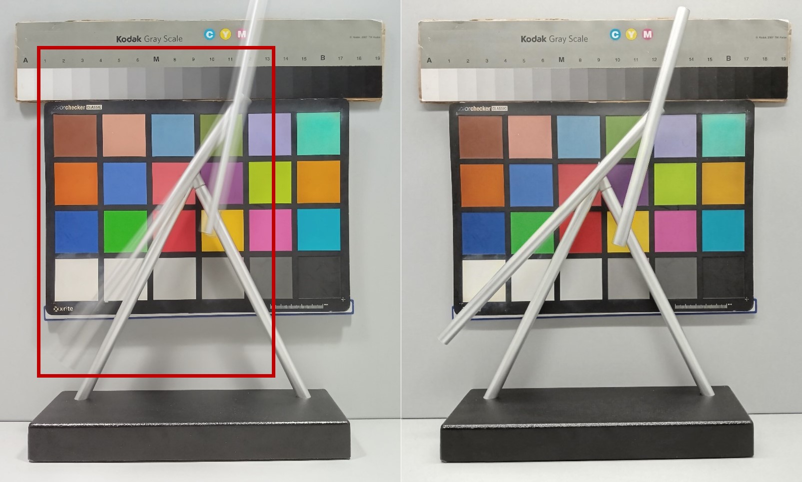
Video Recording: Utilizing multi-frame synthesis, the image sensor alternates between outputting 60fps long-exposure and short-exposure images, which the platform combines to produce a 30fps frame with preserved highlight color and shadow details. While multi-frame synthesis yields noticeable improvements in dynamic range, it significantly increases power consumption, making it unsuitable for prolonged use on devices like smartphones and tablets. Moreover, it tends to produce motion artifacts when capturing moving objects.


Left Image: shot with Multi-Frame HDR (Motion Artifact) Right Image: shot with DAG HDR

GalaxyCore's Patented DAG HDR Technology

GalaxyCore's DAG HDR technology, based on single-frame imaging, employs high analog gain in shadow regions for improved clarity and texture, while low analog gain is used in highlight parts to prevent overexposure and preserve details. Compared to traditional multi-frame HDR, DAG HDR not only increases dynamic range and mitigates artifact issues but also addresses the power consumption problem associated with multi-frame synthesis. For instance, in photography, scenes that used to require 3-frame synthesis are reduced by 50% when utilizing DAG HDR.

Left Image: Traditional HDR Photography Right Image: DAG HDR Photography

GC13A2 Empowers Imaging Excellence with HDR


Empowered by DAG HDR, the GC13A2 is capable of low-power 12bit HDR image output and 4K 30fps video capture. It reduces the need for frame synthesis during photography and lowers HDR video recording power consumption by approximately 30%, while avoiding the distortion caused by motion artifacts.

Compared to other image sensors of the same specifications in the industry, GC13A2 supports real-time HDR previewing, allowing users to directly observe every frame's details while shooting. This provides consumers with an enhanced shooting experience.

GC13A2 has already passed initial verification by brand customers and is set to enter mass production. In the future, GalaxyCore will introduce a series of high-resolution DAG single-frame HDR products, including 32Megapixels and 50Megapixels variants. This will further enhance GalaxyCore’s high-performance product lineup, promoting superior imaging quality and an enhanced user experience for smartphones.

Tuesday, October 17, 2023

ISSW 2024 call for papers announced

Link: https://issw2024.fbk.eu/cfp

International SPAD Sensor Workshop (ISSW 2024) will be organized by Fondazione Bruno Kessler - FBK.
When: June 4-6, 2024
Location: Trento, Italy

Call for Papers & Posters

The 2024 International SPAD Sensor Workshop (ISSW) is a biennial event focusing on Single-Photon Avalanche Diodes (SPAD), SPAD-based sensors and related applications. The workshop welcomes all researchers (including PhDs, postdocs, and early-career researchers), practitioners, and educators interested in these topics.
 
After two on-line editions, the fourth edition of the workshop will return to an in-person only format.
The event will take place in the city of Trento, in northern Italy, hosted at Fondazione Bruno Kessler, in a venue suited to encourage interaction and a shared experience among the attendees.

The workshop will follow a 1-day long introductory school on SPAD sensor technology, which will be held in the same venue as the workshop on June 3rd, 2024.
 
The workshop will include a mix of invited talks and, for the first time, peer-reviewed contributions.
Accepted works will be published on the International Image Sensor Society website (https://imagesensors.org/).

Submitted works may cover any of the aspects of SPAD technology, including device modelling, engineering and fabrication, SPAD characterization and measurements, pixel and sensor architectures and designs, and SPAD applications.
 
Topics
Papers on the following SPAD-related topics are solicited:
● CMOS/CMOS-compatible technologies
● SiPMs
● III-V, Ge-on-Si
● Modelling
● Quenching and front-end circuits
● Architectures
● Time-to-Digital Converters
● Smart histogramming techniques
● Applications of SPAD arrays, such as:
o Depth sensing / ToF / LiDAR
o Time-resolved imaging
o Low-light imaging
o High dynamic range imaging
o Biophotonics
o Computational imaging
o Quantum imaging
o Quantum RNG
o High energy physics
o Free space communication
● Emerging technologies & applications
 
Paper submission
Workshop proposals must be submitted online. A link will be soon made available.
 
Each submission should consist of a 100-word abstract, and a camera-ready manuscript of 2-to-3 pages (including figures), and include authors’ name(s) and affiliation, short bio & picture, mailing address of the presenter, telephone, and e-mail address of the presenter. A template will be provided soon.
The deadline for paper submission is 23:59 CET, Friday December 8th, 2023.
 
Papers will be considered on the basis of originality and quality. High quality papers on work in progress are also welcome. Papers will be reviewed confidentially by the Technical Program Committee.

Accepted papers will be made freely available for download from the International Image Sensor Society website. Please note that no major modifications are allowed.

Authors will be notified of the acceptance of their abstract & posters at the latest by Wednesday Jan 31st, 2024.
 
Poster submission
In addition to talks, we wish to offer all graduate students, post-docs, and early-career researchers an opportunity to present a poster on their research projects or other research relevant to the workshop topics .

If you wish to take up this opportunity, please submit a 1-page description (including figures) of the proposed research activity, along with authors’ name(s) and affiliation, mailing address, telephone, and e-mail address.

The deadline for poster submission is 23:59 CET, Friday December 8th, 2023.

Monday, October 16, 2023

MDPI IISW2023 special issue - 316MP, 120FPS, HDR CIS

A. Agarwal et al. have published a full length article on their IISW 2023 conference presentation in a special issue of MDPI Sensors. The paper is titled "A 316MP, 120FPS, High Dynamic Range CMOS Image Sensor for Next Generation Immersive Displays" and is joint work between Forza Silicon (AMETEK Inc.) and Sphere Entertainment Co..

Full article (open access): https://doi.org/10.3390/s23208383

Abstract
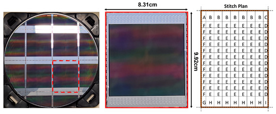
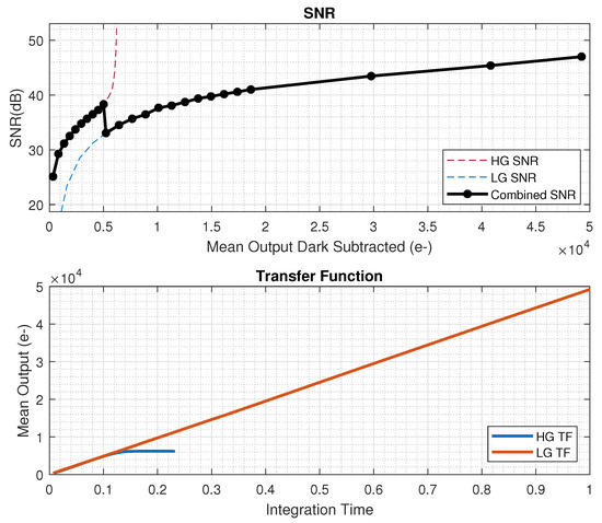
We present a 2D-stitched, 316MP, 120FPS, high dynamic range CMOS image sensor with 92 CML output ports operating at a cumulative date rate of 515 Gbit/s. The total die size is 9.92 cm × 8.31 cm and the chip is fabricated in a 65 nm, 4 metal BSI process with an overall power consumption of 23 W. A 4.3 µm dual-gain pixel has a high and low conversion gain full well of 6600e- and 41,000e-, respectively, with a total high gain temporal noise of 1.8e- achieving a composite dynamic range of 87 dB.

Figure 1. Sensor on a 12 inch wafer (4 dies per wafer), die photo, and stitch plan.


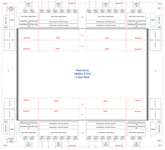
Figure 2. Detailed block diagram showing sensor partitioning.


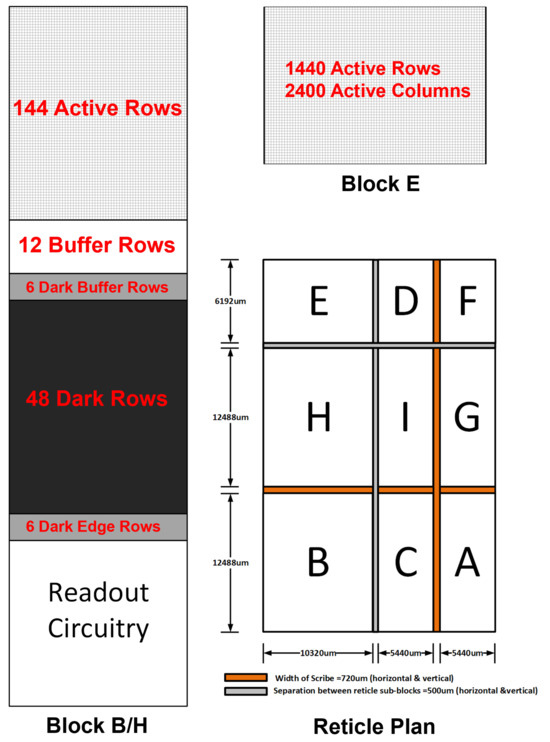
Figure 3. Distribution of active and dark rows in block B/H, block E, and final reticle plan.


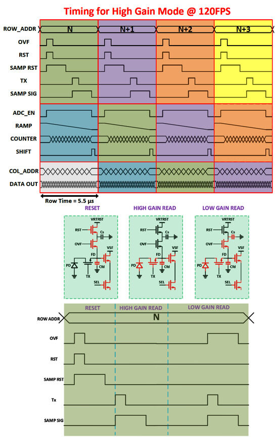
Figure 5. Sensor timing for single-exposure dual-gain (HDR) operation.


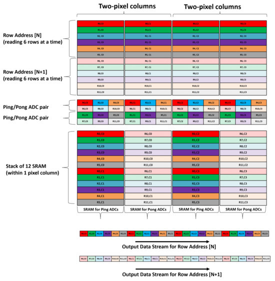
Figure 6. Data aggregation and readout order for single-gain mode.


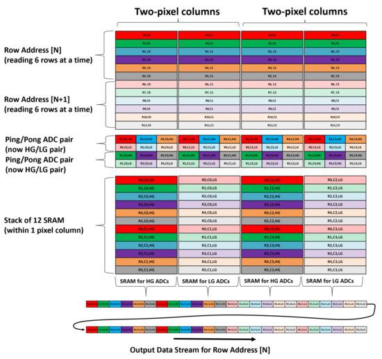
Figure 7. Data aggregation and readout order for dual-gain mode.

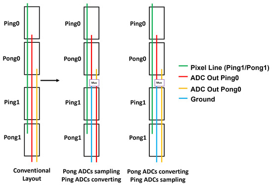
Figure 8. ADC output multiplexing network for electrical crosstalk mitigation.


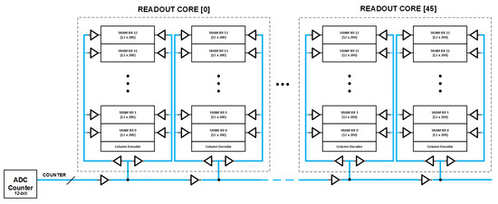
Figure 9. Conventional single-ended ADC counter distribution.


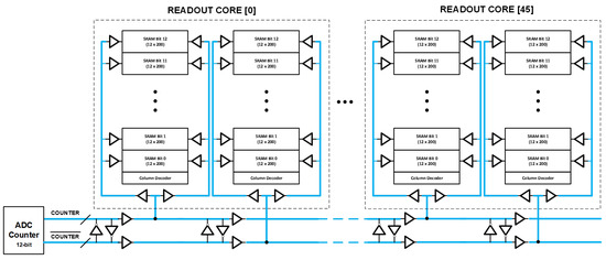
Figure 10. Proposed pseudo-differential ADC counter distribution.


Figure 11. Generated thermal map from static IR drop simulation.

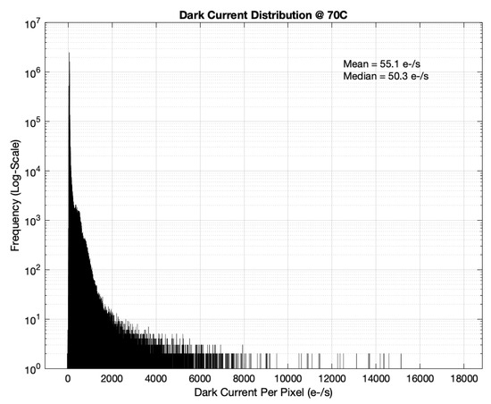
Figure 12. Measured dark current distribution.

Figure 13. SNR and transfer function in HDR mode.


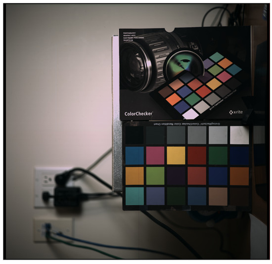
Figure 14. Full-resolution color image captured in single-gain mode at 120 FPS.