Lists

Friday, September 28, 2012

Image Sensors 2013 Calls for Papers

PRLog: Image Sensors 2012 (London, UK conference) announcs the Call for Papers for IS2013. It seems that the conference has the new owner, Smithers.

The IS2013 is planned to cover the following applications in image sensor technology:

  • Automotive imaging
  • Digital Still Cameras
  • Machine Vision
  • Time-of-flight and 3D imaging
  • Metrology
  • Low light level imaging

The conference will also feature an 'Expert Panel' session to discuss some of the pressing issues facing the sector, and an 'Innovation Platform' session to give academics, spin-outs, and SMEs an opportunity to present their latest innovations to the audience.

A short summary of the proposed presentation (max 500 words), plus a speaker biography can be submitted to rstead@smithers.com by 26th October 2012.

Thursday, September 27, 2012

Apple Acquires TFT Image Sensor Patent

PatentlyApple reports that Apple has purchased TFT image sensor patent US7,773,139 titled "Image sensor with photosensitive thin film transistors". The three Oregon-based engineers that invented this process are Willem den Boer, Tin Nguyen and Patrick Green.

Wednesday, September 26, 2012

Sony Abandons "RGBW Coding" in Stacked Sensors

Sony announced announced specification changes to its Stacked CMOS Image Sensors IMX135 and IMX134 and the camera modules based on these sensors, IU135F3-Z and IU134F9-Z, which are scheduled for phased launch starting January 2013.

Sony will switch their color coding to a RGB instead of originally announced "RGB-W coding", as it has failed to meet "certain conditions of Sony's image quality standards".

Sony also changed the sensitivity specs (typical value F5.6): 92mV (Green pixel) and 127mV (White pixel) changed to 84mV (Green pixel).

Tuesday, September 25, 2012

Digitimes: Samsung Gains Market in China

Digitimes quotes Samsung distributor in China expecting revenue increase in September on orders for Samsung's image sensors from local smartphone makers.

Some local smartphone vendors are said to be switching to Samsung image sensors as Sony's and Omnivision's production capacities have been fully booked by Apple, according to Digitimes' sources. The distributor expects to deliver up to five million sensors to these customers in September, according to Digitimes' sources calculations.

Monday, September 24, 2012

More Details on Panasonic 1.12um SmartFSI Pixel

It appears that most of the previous articles quote Panasonic PR in Japanese from Sept. 20. The PR has few other interesting claims:
  • Panasonic contemplates release of 14MP and 16MP models based on the same 1.12um SmartFSI pixel.
  • The angle of incidence is quoted as 40deg due to advanced light guide (see figure below)
  • The module height can be reduced down to 70% of that with BSI sensors
The lightpipe figure has all the explanation in Japanese, embedded in the image. Google translator is helpless here. It would be great if somebody can translate it:


Panasonic also published a higher resolution view of microlens array:


Update: Thanks to TN for translating the picture:

Saturday, September 22, 2012

Panasonic to Launch 1.12um FSI Pixel

Tech-On published more details about Panasonics's oncoming 13MP sensor for smartphones. The sensor format is 1/3.06-inch, meaning the pixel size of about 1.1um. It belongs to its SmartFSI family. This makes Panasonic the only company talking about a non-BSI 1.1um pixel.

The new pixel sensitivity is said to be the highest in the industry at 3,230e-/lx/sec/sq.um. Panasonic claims it has improved S/N ratio by a factor of two. A "light-concentrating structure" improves the new pixel's color reproducibility and angular response.

Another three new features of the sensor, as quoted by Tech-On:

  • high-sensitivity photo diode: wide, deep photo diodes in small pixels
  • microfabrication technology, which reduces parasitic capacitance for improving the sensitivity of in-pixel amplifier and reducing the noise of transistor
  • optimal matching design technology for the lens of camera module and the light-concentrating structure developed by Panasonic

Chipworks: iPhone 5 Primary Camera Sensor Made by Sony

While the initial look has not revealed the Apple iPhone 5 primary sensor part number, Chipworks found "a lonely little "SONY" mark on the sensor. The measured pixel size is 1.4um, same as in iPhone 4S:


The front camera's sensor has been identified as Omnivision's:

Friday, September 21, 2012

Ambarella Announces 4K IP Camera SoC Family

Ambarella introduces S2,a security IP camera SoC with support for the new 4K Ultra HD video standard, based on a Dual Core ARM Cortex-A9 CPU and a high-performance video engine that delivers multi-stream H.264 encoding up to 4K (3840x2160p30) resolution. Hardware analytics acceleration enables cameras to analyze video content and make intelligent decisions based upon it. Using low-power 32nm process, the S2 delivers 1080p60 encoding in less than one Watt and 4K video encoding in less than two Watts.

"By delivering 4K video and multi-core CPU performance in a 32nm low-power design, Ambarella is enabling high resolution video in compact camera form factors," said Fermi Wang, President & CEO of Ambarella.

The S2 family provides an array of IP camera design choices. The family is comprised of software and pin-compatible SoCs that range in performance from 1080p45 encode with a 500 MHz dual-core CPU to 4K Ultra HD encode with a 1 GHz dual-core CPU. Its advanced features include panoramic lens de-warping, hardware face detection, digital PTZ and EIS. The Linux based SDK supports a wide range of image sensors and enables features such as WiFi connectivity, cloud services, local SD Card recording and transcoding. The SDK also offers comprehensive 3A and image tuning tools for customization.

S2 Feature Summary:
  • Image Sensor Pipeline with high-speed SLVDS/MIPI®/HiSPi™ interfaces, up to 32 Megapixel (MP) sensor resolution.
  • Wide Dynamic Range (WDR) with multi-exposure fusion to improve video in high-contrast lighting conditions.
  • Advanced 3D noise reduction with de-ghosting to enhance low-light performance.
  • 4K video (3840x2160p30 or 1920x1080p120) H.264 encoding to support the new Ultra HD standard. Multi-streaming to enable independent resolutions, frame rate and quality. Support is also offered for video transcoding and low-latency encoding.
  • Dual Core ARM Cortex-A9 CPU with NEON and a 512 KB L2 cache provides headroom for customers’ applications, as well as enhanced power efficiency and real-time performance compared to single-core architectures.
  • Analytics hardware acceleration for efficient processing of tasks like object tracking, trip zone perimeter control and intelligent motion detection.
  • Real-time hardware-accelerated de-warping for 180/360 degree panoramic lenses.
  • AES/3DES/SHA-1/MD5 encryption engines.
  • Interfaces includes32-bit DDR3L, Gigabit Ethernet, USBG 2.0 host and device, HDMI®, SDXC SD™ Card, and dual sensor interfaces.
The S2 family of SoCs is available now for qualified customers.

Thursday, September 20, 2012

Panasonic to Launch 13.4MP Sensor for Smartphones

Jiji Press quotes Panasonic announcing today that in December it will launch production of a the new 13.4MP image sensor for smartphones and other mobile devices. The sensor is said to use "semiconductor microfabrication technology to curb image noise". It is going to be one of the thinnest image sensors in the industry so it can be used in very thin smartphones and tablets, Panasonic said.

Pixart Sales for Nintendo Wii U to Reach 20% of Total

Digitimes expects Pixart to report Q3 results meeting its guidance for a 40-50% on-quarter growth, fueled by Nintendo's Wii U console sensors.

Shipments of sensors for Wii U are expected to reach NT$200 million (US$6.8 million) or 20% of Pixart's total sales in the third quarter, according to Digitimes' sources. The Wii's shipments are likely to peak in October and then begin slowing down due to fierce competition in the gaming sector and a lack of new attractive software delivered by the Wii U, the sources commented.

Wednesday, September 19, 2012

PTC Data Sources

Albert Theuwissen discusses possible ways to get data for PTC graph in his latest post of "How to Measure..." series.

Tuesday, September 18, 2012

CMOSIS Sensor in "Leica M" Rangefinder

CMOSIS announced that it has developed a 24MP HDR full-frame sensor exclusively for Leica Camera AG geared to an important volume market. The new "Leica M" digital camera launched at Photokina 2012 incorporates the full-custom CMOSIS "Leica MAX 24MP CMOS Sensor" with active area of 36 x 24 sq.mm, aka the full-frame 35mm format. The sensor is the first milestone in a long term, strategic cooperation between Leica Camera AG and CMOSIS.

"This is the first time that a CMOS image sensor for a 35mm high-end camera was designed, and is manufactured, in Europe for a European customer," said Guy Meynants, CTO at CMOSIS, Antwerp, Belgium. "Apart form the ceramic IC package the Leica MAX 24MP CMOS Sensor is a 100-percent European product."

The new sensor features 6um pixels and is made by STMicroelectronics in Grenoble, France, using 300mm wafers in their IMG175 CIS technology. STM's 110nm frontend and 90nm backend CIS technology with copper metallization was originally developed for CMOS image sensors with 1,75um pixels for mobile phones and other consumer applications. The large die size, larger than the reticle size, requires the use of one-dimensional stitching.

The 6um pixel has a linear full well capacity of ≥40,000e- and a linear DR close to 76dB. Pixel data are digitized by patented low-power, high-speed 14-bit column ADCs. The sensor features an electronic rolling shutter with global reset and noise cancellation through both analog as well as digital correlated double sampling (CDS) resulting in low temporal and spatial noise and non-uniformities.

Special care was taken in the sensor development to reduce crosstalk between neighboring pixels for a wide range of incident light angles. The sensor reduces spatial crosstalk by its very thin stack from color filters to photodiodes. Microlenses with a strong curvature and high top height focus the incoming light rays in the center of each pixel's photodiode. The resulting low angular sensitivity of the QE at high ray angles was achieved by the particular features of STM's 110/90nm CMOS process. This allows the "Leica M" to accept the full range of high-quality lenses in the camera system, which includes wide-angle, large aperture lenses, at their full optical performance.

The full resolution frame rate is 5fps. The 24MP sensor also allows Leica to offer, for the full HD video recording and a live preview on an M-model camera. Power consumption of the sensor chip at full speed and resolution is specified at 700 mW.

It is housed in a 78-pin ceramic package covered by a customized glass with anti-reflective coating and near-infrared cut-off filter.


Update: EETimes Europe published an explanation picture on large angle of incidence in CMOSIS pixels:


Update #2: Electronic Specifier published a complete set of facts about the CMOSIS-Leica sensor.

Aptina Announces 1-inch 10MP Sensor for Bridge and Mirrorless Cameras

Business Wire: Aptina announced the 1-inch 10MP AR1011HS digital camera image sensor aimed to high quality bridge and mirrorless cameras and targeting Tier-1 camera OEMs. The sensor is based on 3.4um pixels "delivering uncompromised low light and bright light scene image quality". Its high-speed architecture is capable of reading full 10MP resolution at 60fps, and enables a variety of video modes, including broadcast quality quad HD, oversampled 1080p for True HD resolution, 1080p video at 120 fps, and additional high frame rate modes for slow motion playback.

"Image quality and speed are the two things this market cannot compromise on. Tier-1 OEMs competing in this market are looking for increasingly versatile solutions to meet the demand for speed and performance, and this sensor provides both," said Sandor Barna, VP and GM of Aptina’s Consumer Camera business.

The AR1011HS DR-Pix pixel is said to deliver both high-pixel sensitivity for low-light imaging, and high-pixel capacity for bright outdoor scenes. The new sensor uses 24-lane HiSPi High Speed Serial Pixel Interface for fast data transfer.

The AR1011HS is currently sampling in limited volumes and will be in mass production in Q1CY13.

Aptina Launches 1.25um BSI Pixel in 18MP Sensor

Business Wire: Aptina announced 1.25um BSI pixel-based AR1820HS sensor for the consumer digital camera and DV market. The new sensor packs 18MP is 1/2.3-inch optical format.

The AR1820HS utilizes Aptina's A-PixHS technology, which brings Aptina’s BSI pixel technology together with advanced high-speed architecture.

The native 18MP resolution can be read out at up to 24fps for high-speed burst still image capturing. In video modes, the sensor can output a 16:9 aspect ratio, full field-of-view 14MP at 30fps and a binned 8MP at 60fps. This oversampled image readout enables superior resolution, noise performance, and cleaner overall video. Additionally, over-sampled video provides extra area for electronic image stabilization (EIS) and steady digital zooming. The AR1820HS pixel summing capability provides the camera designer with the option of faster 1080p60 and 1080p120 video modes, or lower power consumption video options. The AR1820HS uses 8-lane HiSPi serial interface (800Mbps per lane).

"The AR1820HS image sensor and Aptina’s A-PixHS Technology provide OEMs with the combination of exceptional image quality and the high speed capture features needed to create a compelling new generation of consumer camera products," said Sandor Barna, VP and GM of Aptina’s Consumer Camera business.

The new AR1820HS improves on MT9F002 14MP sensor that has had with Tier-1 consumer DSC, DVC, and Sportscam markets. The AR1820HS delivers improved low ISO speed (outdoor) performance, high-ISO speed (low light) performance, lower structured noise, and better angular response than the MT9F002 14MP sensor.

The AR1820HS is currently sampling in limited volumes and will be in mass production in Q3CY13. Aptina shows a downsampled image from the sensor:

Monday, September 17, 2012

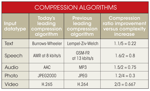
Compression Limits Nearing

Electronic Design published an article on compression algorithm evolution and its limits by Al Wegener, CTO and founder of Samplify Systems, Santa Clara, CA. It looks like still image compression does not have much potential to improve in the coming years, while video compression's future looks better:

LFoundry Announces 90nm CIS Process

PRWeb: Thanks to the materialization of several large-scale projects, LFoundry plans to invest a total EUR 25 million in R&D and innovation projects over the next three years.
Its latest developments include LF110 PDK (Process Design Kit) for the 110nm Aluminum process with an optional 90nm image sensor module. The PDK was released in May 2012 and early stage MPW (multi project wafer) are running in the line.

LFoundry is an analog and mixed signal foundry with 200mm manufacturing located in Rousset, France and Landshut, Germany with a wafer capacity of about 20,000 wafers/month. The former reports claimed that its Germany fab is insolvent.

Update: EETimes says that the €25M investment is intended for the fab in France , while the Landshut, Germany facility has been shut down.

Sunday, September 16, 2012

ULIS IR Imaging Videos

Grenoble area, France-based ULIS published few videos on IR imaging usability in different applications. ULIS develops amorphous silicon IR imagers.

Vimeo video on automotive applications:

ULIS thermal imaging sensors for transportation applications from ULISCompany on Vimeo.


Video on surveillance and security:

ULIS thermal imaging sensors for surveillance and security applications from ULISCompany on Vimeo.


Few other videos can be found on ULIS' Vimeo channel.

Friday, September 14, 2012

Pixpolar MIG Sensor for Security Apps

Pixpolar published a post on advantages of using its MIG pixel in security and surveillance applications.

At low light illumination, the frames in video stream might need to be combined to get a sufficient SNR for identification purposes. In most sensors, the frame addition also adds the read noise, so the SNR grows as square root of the number of frames. Due to the non-destructive read capability, Pixpolar's MIG pixel can be reset once per many video frames. Then the video frames are extracted by subtraction, while the integrated long frame between the resets carry just one-time read noise component.

Pixpolar's demo of the idea is marred by the fact it assumed the CIS sensor to have lower QE than its MIG pixel (not sure why), but it illustrates the approach:

Simulation result presenting the signal-to-noise ratio enhancement when multiple frames are merged together in high end CIS and MIG technologies. The simulation was done for low intensity NIR illumination (50 photons / second in brightest areas). QE in CIS was assumed to be 28 % and in MIG 70 %. The read noise in both sensors was assumed to be 1 e-. Dark current in CIS was 0 e-/s and in MIG 1 e-/s. The frame rate was 25 fps and in total 50 frames was merged together.

Sanyo CCD Patents Up for Sale

UBM TechInsights is offering for sale a portfolio of 198 ON Semiconductor patents, originally patented by Sanyo. Out of the 60 US patents in this portfolio, 18 are devoted to CCDs:

"Lot #2 includes Image sensors (CCD), sensor power saving, signal processing crosstalk suppression, as well as a patent on using an LCD as a controllable lens cover. The fabrication patents relate to supplying power to a CCD cell using silicide lines, fabricating photo diodes with improved sensitivity, forming micro-lenses over the pixel array, and using dummy metal traces to reflect light into corresponding pixels."

Some of them are commented by Techinsights in the presentation document I received by email:


Whoever is interested can inquire UBM Techinsights (contact emails are available on request).

Thursday, September 13, 2012

Assorted News: Ambarella, e2v, PCIe over MIPI

e2v announces that it will provide sensors for the next generation of focal plane imager in the SPring-8 Angstrom Compact free electron Laser (SACLA), an X-ray Free-Electron Laser (XFEL) located in Hyogo Prefecture, Japan.

e2v’s imaging sensors detect the X-rays scattered by the scientific samples in the XFEL beam. From these scattered X-rays scientists will be able to “see” the atomic structure of proteins and other nano-scale structures.

Ambarella has filed for NASDAQ IPO under the symbol AMBA. Now the company has reported its Q2, 2012 results. The quarterly revenues rose 7% sequentially to $27.9M primarily due to the seasonality of the camera market, though sales rose 26% year-over-year as well. Net profit margin reached its highest point in the past three years at 19%, increasing from 4% in the second quarter of 2011. Ambarella has booked $107M in sales for the 12 months ended July 31, 2012.

EETimes reports that PCI Special Interest Group and MIPI Alliance signed a deal to offer PCIe protocol on top of MIPI M-PHY signalling layer. "We are making PCI Express mobile friendly," said Brian Carlson, vice chairman of the MIPI Alliance. M-PHY was first defined in April 2011 at 1.25 Gbits/s, an update released in June 2012 runs at 2.9 Gbits/s and a third generation coming next year will hit up to 5.8 Gbits/s.

Aptina Invests into Multi-Array Gigapixel Future

Business Wire: Aptina partnered with the Duke Imaging and Spectroscopy (DISP) for the AWARE gigapixel camera program as an image sensor supplier. The AWARE program is funded by DARPA and aims to build a a wide FOV gigapixel camera out of array pf Aptina's 14MP sensors. The camera is said to have five times the resolution of the human eye.

David J. Brady, the Michael J. Fitzpatrick Professor at Duke University leads DISP and spearheaded the AWARE-2 program, selecting Aptina to supply with modified MT9F002 14MP sensors and camera system support. "We chose Aptina’s 14-megapixel sensor because it provided the resolution, quality and speed required by the project," said David Brady, project lead.

Also Aptina is conducting an independent R&D on the multi-array concept and extending the idea of capturing images using multi-sensor and multi-camera solutions. "While the AWARE-2 camera uses a large array of individual sensors each in a micro-camera, we are committed to the miniaturization of the multi-array concept, achieved by integrating multiple imaging arrays within an individual sensor chip. These miniaturized single-chip multi-array solutions could revolutionize the imaging industry, enabling exciting new features and applications," said Bob Gove, President and CTO at Aptina.

Aptina’s work in this area includes various prototyped multi-array sensors including sensors containing imaging arrays from three to 25 individual imaging arrays. Aptina envisions a range of future applications to include smartphone cameras with exceptional color performance, depth mapping for gesture recognition and gaming, security, medical and military uses. Multi-array cameras provide a new direction from traditional cameras that opens the possibility for extremely flexible designs for both normal photography and computer vision for new human interactive systems.

Example images from AWARE web site:

8MP Cameras Remain Smartphone Mainstream in 2H 2012

Digitimes: Largan CEO Lin En-ping says that he expects 8MP cameras remain in the smartphone mainstream for 2H 2012, as 10MP lenses are currently too expensive. At 8MP node, smartphone vendors ask for the slimmer profile and larger aperture. 5P element lenses are used for most of the 5MP and 8MP products.

Wednesday, September 12, 2012

Pixart Sales, Margins Growing

Digitimes sources expect that Pixart continues to supply sensor bars for the new Wii U, to be launched on Sept. 13.

Pixart has reported revenues of NT$333M (US$11.2M) for August, up over 40% on month and 24.6% on year basis. The August figures are the company's highest in two years.

Shipments of sensors for gaming consoles and optical finger mice (OFM) will ramp up revenues by 40-50% sequentially in Q3, the company said earlier. Pixart posted revenues of NT$677M in Q2.

Pixart expects its gross margin to grow to 43-45% in Q3 2012 compared to a range of 35-41% recorded in the previous seven quarters, thanks to a more favorable product mix.

Eedoo Console Sales Goals

TechInAsia: Eedoo CEO Jack Luo said that he expects CT-510 console to have some "tens of thousands" of units by the end of its first fiscal year (March 31, 2013). This is a modest goal for a device that cost $15 million in R&D alone. For comparison, Microsoft sold about 18 million Kinects (worldwide) in its first year of sales.

Tuesday, September 11, 2012

Intel Perceptual Computing Demoed on Softkinetic Camera

SoftKinetic announces that its 3D DepthSense camera and middleware for close-range gesture tracking will be included in the Intel Perceptual Computing Software Development Kit 2013 (SDK) Beta announced and demonstrated at the Intel Developer Forum 2012 today.

VentureBeat says that Intel believes that the close-range gesture-recognition that is able to detect finger moving is a way to go for controlling ultrabooks.

"SoftKinetic is a pioneer and leader in the field of 3D gesture recognition who is helping us to make our vision of natural, interactive user experiences a reality," said Achin Bhowmik, Director of Perceptual Computing at Intel. "Gesture-based interaction enables humans to interact in a natural, intuitive way with their computer systems."

The 3D camera itself bears Creative Labs logo, although the basis of the design is SoftKinetic DS325, or so I was told:


The camera has RGB and Depth frames sync, 30fps speed, depth range of 0.5ft to 3.25ft (15cm-1m), FOV 73deg and powered by a single USB2 port with power less than 2.5W. The camera become available, starting October, 2012. The cost of the camera will be available for developers in October 2012 for $149.00 plus tax and shipping. The commercial release is planned for the first half of 2013.

Mitch Reifel, Softkinetic VP of Sales, says: "the idea is that this technology starts as a peripheral and the technology will improve, get smaller z-height and lower cost to integrate [into the Ultrabook lid - ISW]. We will be announcing another major partner in 4Q that will help us realize this, so more info will be coming soon."

Here is a picture of what Intel showed at their forum:


Update: EETimes: Intel announces a $1M prize for the best user interface innovations using the new perceptual computing developers kit.

Pelican Imaging Expands its Management Team

PR Newswire: Pelican Imaging, a venture-backed computational imaging startup, has appointed a new CEO and new VP Engineering. Christopher "Chris" Pickett will serve as Pelican Imaging's president and CEO, while Purnam Sheth will take on the role of VP Engineering.

Chris Picket has an extensive experience in technology licensing. Most recently, Pickett was SVP of corporate licensing for Rambus, which he joined as part of the acquisition of Global Lighting Technologies, where he was president of the licensing division. Before joining Global Lighting Technologies, he was EVP of licensing at Tessera.

Most of Purnam Sheth's experience is in networking and mobile, not directly related to imaging.

"Pelican Imaging is poised for explosive growth. The company's technical expertise, coupled with experience that both Chris and Purnam bring to the table, position Pelican to launch a new era in the way people interact with the images and video they capture," said Barry Schiffman, executive managing director at Globespan Capital Partners and a member of Pelican's board of directors. "Pelican has ambitious plans under way on several fronts. These additions to its leadership team prepare the company for establishing new partnerships and channels that can broaden adoption of its technology."

"Pelican's technology is receiving incredible response from a variety of consumer platforms that utilize cameras. It is clearly a game changer for a variety of camera markets and promises a much thinner module solution, as well as better low light performance, which will help to make phones and tablets even thinner, more advanced and able to offer the user a host of post capture editing functions that are difficult or impossible with current camera technology," said the new CEO Chris Pickett.

Teledyne-DALSA Announces 60MP Medium-Format CCD

Marketwire: Teledyne-DALSA's new 60MP FTF9168 CCD is said to offer the highest resolution available in the industry today within a 645 optical format that can be imaged using commercially available lenses. Available in both RGB-Bayer color and monochrome versions, the FTF9168 CCDs are targeting the resolution-demanding applications like fabric and artwork reproduction, document scanning and aerial photogrammetry. The sensor is based on 6um pixels and has the maximum frame rate of 1.4fps.

FTF9168 features:

  • Very large optical format (54 x 40 mm2)
  • 60 million active pixels (8956H x 6708V)
  • >95% fill factor
  • Micro lenses with wide angular response
  • High sensitivity & dynamic range (>70dB)
  • Data rate up to 25 MHz per output (4 outputs)

"With our internal wafer foundry, we can control the entire process from design to delivery, offering both the ultimate in performance tuning and security of supply," said Jelle de Jong, Director of Marketing and Sales at Teledyne DALSA in Eindhoven. "The FTF9168 contributes to our continuing history of excellence and is the highest-resolution large optical format sensor available on the market today."


DALSA publishes a complete datasheet simultaneously with the announcement - quite a rare occurrence in the industry. The QE graphs are among the officially presented data:


With the new sensor, the large format CCD lineup from DALSA spans from 22MP to 60MP:

Sunday, September 09, 2012

Noise Measurement Caveats

Albert Theuwissen discusses potential pitfalls in image sensor noise measurements, quite many of them.

Saturday, September 08, 2012

Delft University HDR and GS Sensor Theses

Delft University published MS thesis by Yang Liu "The Design of a High Dynamic Range
CMOS Image Sensor in 110nm Technology
", apparently based on CMOSIS work done in cooperation with CMOSIS. The sensor is made in 0.11um process with pixel size of 4.8um. The 6T pixel has 3.1e- noise and 84.5dB DR:


Two floating diffusions FD1 and FD2 are needed to provide high and low conversion gain paths for low light and strong light signals. The maximum charge is limited by either FD2 capacity or PD well. The reported pixel full well is 51750e-.

In order to reduce the image lag, the two transfer gates are placed in the corners on the same side:


Another recently published thesis based on CMOSIS global shutter work is "The Design of a Global Shutter CMOS Image Sensor in 110nm Technology" by Xiaoliang Ge. The thesis has many interesting details on shrinking CMOSIS 8T global shutter pixel to 4.8um in 0.11um process:


Thanks to TH for the link!

Friday, September 07, 2012

Gesture and Face Recognition at Next Week's IDF

Venture Beat, EETimes: Intel is to show its new camera-related technologies at Intel Developer Forum (IDF) in San Francisco next week. David Perlmutter, EVP and Chief Product Officer at Intel, is to introduce the idea of "perceptual computing," which will focus on computer controls beyond touchscreens and keyboards. Intel is pouring a lot of investment into technologies that will debut this year and next, including the "interactive space between you and the screen," said an Intel spokesman. The technologies include gesture recognition, face recognition, cameras and sensors, and other ways to make your intentions known to a computer.

Thanks to MR for the link!

Market Pulse

PR Newswire: MIC (Market Intelligence & Consulting Institute), an ICT industry research institute based in Taiwan, estimates the camera phones' share of the global mobile phone market to stand at 83.2% in 2012 and increase to 84.8% in 2013. The overall camera phone market volume is expected to see a 10.5% year-on-year growth in 2013 to 1.63 billion units.

Worldwide mobile phone CMOS image sensor market volume is estimated at 2.089 billion units in 2012, growing 21.1%, and market volume share of image sensors used for sub-camera modules [not sure what's sub-camera - ISW] in overall market will hit 29.2%. The worldwide mobile phone CMOS sensor market volume will increase by 17% in 2013, reaching around 2.44 billion units.

Research In China's Global and China CMOS Camera Module Industry Report, 2011-2012 says that Apple generated great advertising effect when iPhone adapted Sony sensors a year ago. Many other customers have been attracted to order CMOS sensors from Sony. In 2011, Sony enjoyed a market share of around 12% in mobile phone CMOS sensor industry, and the figure in 2015 is expected to be 30%.

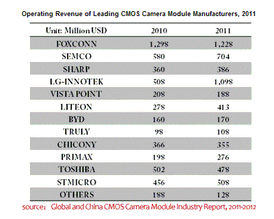
In the camera module space, benefiting from "Apple effect", the business of LG Innotek, as the major provider of camera module for Apple, grew by more than 100% compared to less than 10% in the entire industry in 2011. The three camera module suppliers approved by Apple are LG Innotek, Sharp, and Primax:

Thursday, September 06, 2012

Chipworks: Sony Sensor Inside Nikon D800 DSLR

Remember Nikon D800 DSLR sensor tested by DxO Labs and proclaimed "the new king of DxOMark"? The new Chipworks report reveals that its 36.3MP/4fps CMOS sensor is made by Sony.

Thanks to EF for the link!

DxO Labs Improves its Camera Analyzer

DxO Labs announces its DxO Analyzer v5, a camera and sensor characterization suite. Its new features include enhanced video measurements, 3D camera measurements, image stabilization quality and more. The new features are presented by Nicolas Touchard, DxO Labs’ VP of Marketing, Image Quality Evaluation in this Youtube video:

ST 65nm BSI Process to be Openly Available through UMC

PR Newswire, EETimes: UMC joins forces with ST to develop 65nm BSI process. The partnership follows upon the two companies' success to port ST's FSI processes to UMC's 300mm Fab 12i in Singapore. The 1.1um pixel BSI process, which will also be developed at Fab12i, will be available as an open platform for customers through a licensing agreement with ST.

Po-Wen Yen, Senior Vice president of 12-inch Operations at UMC said, "We are happy to extend our relationship with our long-time partner STMicroelectronics through this co-development effort. This agreement is consistent with UMC's open collaboration strategy to deliver customer-driven foundry solutions to address ever evolving market requirements. We look forward to further strengthening our comprehensive technology portfolio with this CIS BSI process."

"ST's previous successes in imaging technologies with UMC gives us great confidence in the development of this next-generation image-sensor process technology with UMC," said Eric Aussedat, Corporate Vice President Imaging, Bi-CMOS, ASIC and Silicon Photonics Group.

Initially, the new process is targeted to fast-growing applications such as smartphone, tablet, high-end surveillance, and DSC/DSLR. The long lifetime expectancy of the BSI process should help it to be adopted for automotive and industrial fields in the coming years.

Thanks to RF for sending me the link!

Tuesday, September 04, 2012

Nokia Files for Graphene Image Sensor Patent

UnwiredView.com noticed that USPTO published Nokia patent application US20120205518:

"Sensing of Photons" by Martti Voutilainen, Markku Rouvala, and Pirjo Pasanen.

The sensor consists of multiple light-sensitive layers of graphene connected to the gates of graphene amplifying FET 106 and 107 and to source of graphene reset transistor 108. Fig. 1 shows a horizontal structure of the pixel, while Fig. 2 shows the vertical cross-section together with RGB color filters 221-223:

Monday, September 03, 2012

Toshiba Publishes 1.12um BSI Pixel Claims

Toshiba Review published Science and Technology Highlights 2012 with few words about the status of its 1.12um BSI pixel development. Thoshiba claims to be the first company in the world that mass produces 1.12um pixel sensors, as of Dec. 2011.

The new 8MP image sensor is said to achieve 125% higher sensitivity per unit area as compared with 1.4um FSI pixel sensor [probably meant to be 25% improvement, rather than 125%]. The "partially introduced" 40nm process helps to increase the PD area and achive 118% saturation charge per unit area. The sensor also features "optimization of the transistor sharing method and photodiode isolating structure" to increase speed and reduce crosstalk and noise.

The 8MP sensor has a speed of 30fps at full resolution or 60fps in 1080p video mode. It also includes HDR function. This description appears to be close to the previously announced T4K05 spec.