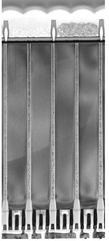
IEEE Spectrum has published an article about a race towards the smallest pixel size. The article is titled "Samsung and Omnivision Claim Smallest Camera Pixels" where both companies have claimed to achieve ~0.6 micron pixel pitch for their CMOS image sensors.
Last month, two companies said they have reached the next stage in shrinking the pixels on CMOS camera chips. Both Santa Clara-based Omnivision and South Korea's Samsung claimed pixels with a pitch of just 0.56 micrometers (measured from the center of one pixel to the center of the next), which is about as large as the wavelength of green light.
One challenge with such shrinking pixel sizes is the well capacity. The article continues...
Samsung's 0.64-micrometer device can hold the equivalent of 6000 electrons ... . Shrink that area down to 0.56 micrometers without changing anything and you're left with only 3400.
Another challenge is crosstalk...
Seeking to strengthen the barrier against stray light... Samsung went to the extreme—an air gap.
...there will be even tinier pixels in the future.
... Samsung engineers went on to add.
Where are we headed? Where will this race end? Are we converging towards single-photon cameras pixels with ultra-low well capacities of a single-digit photo-electrons?

Full article here: https://spectrum.ieee.org/cmos-image-sensor-pixel
[Text in italics is verbatim from the original article. Text not in italics are this blog post author's comments and musings.]
As posted by Albert several times before - it is absolutely fascinating how this DTI structures can be fabricated. the walls are about 1 wavelength of green light apart from each other. Probably 50-70nm wide and a few um deep...
ReplyDeletePlus: thanks to Atul and the other new authors - it is great that image sensors world blog keeps being active!
Maybe new for CIS, definitively nothing new for NAND or DRAM. Samsung has lot of experience in these areas, if they are smart, and I think they are, they are sharing the knowledge.
DeleteDefinitively a fascinating exercise, does it really improve the image quality?
ReplyDeleteyou start with 200 mega(small) pixel to get an 8k video or 16mpixel still photo, is it really better than a 40 mpixel of nicely sized pixels?
Dimensions are comparable to wavelengths, quantum effect may arise
I'm glad to see the blog alive again, a precious resource through my adventure (and career) in the image sensor world.
Thanks for the article! I remember someone wrote a digital zoom capability of very high pixel count sensor is one advantage, but I wonder if it is true and what could be other pros.
ReplyDeleteSamsung showed the MTF value of Tetracell(?) increases until the pitch size is about 0.4um on '21 IISW. I am so happy to see the blog again.
ReplyDelete