Photonics magazine has a new article about Pi Imaging Technology's high resolution SPAD sensor array; some excerpts below.
As the performance capabilities and sophistication of these detectors have expanded, so too have their value and impact in applications ranging from astronomy to the life sciences.
As their name implies, single-photon avalanche diodes (SPADs) detect single particles of light, and they do so with picosecond precision. Single-pixel SPADs have found wide use in astronomy, flow cytometry, fluorescence lifetime imaging microscopy (FLIM), particle sizing, quantum computing, quantum key distribution, and single- molecule detection. Over the last 10 years, however, SPAD technology has evolved through the use of standard complementary metal-oxide-semiconductor (CMOS) technology. This paved the way for arrays and image sensor architectures that could increase the number of SPAD pixels in a compact and scalable way.
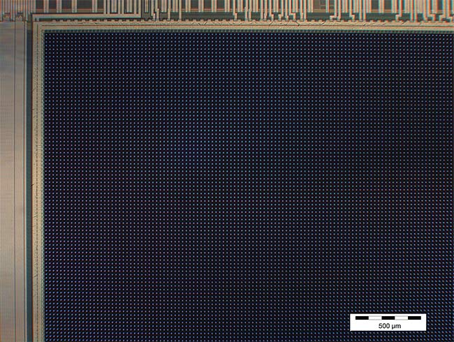
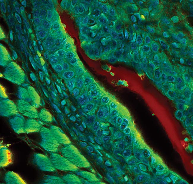
Compared to single-pixel SPADs, arrays offer improved spatial resolution and signal-to-noise ratio (SNR). In confocal microscopy applications, for example, each pixel in an array acts as a virtual small pinhole with good lateral and axial resolution, while multiple pixels collect the signal of a virtual large pinhole.
Challenges:
Early SPADs produced as single-point detectors in custom processes offered poor scalability. In 2003, researchers started using standard CMOS technology to build SPAD arrays. This change in design and production platform opened up the possibility to reliably produce high-pixel-count SPAD detectors, as well as invent and integrate new pixel circuity for quenching and recharging, time tagging, and photon-counting functions. Data handling in these devices ranged from simple SPAD pulse outputting to full digital signal processing.
Close collaboration between SPAD developers and CMOS fabs, however, has helped SPAD technology overcome many of its sensitivity and noise challenges by adding SPAD-specific layers into the semiconductor process flow, design innovations in SPAD guard rings, and enhanced fill factors made possible by microlenses.
Applications:
Research on SPADs also focused on the technology’s potential in biomedical applications, such as Raman spectroscopy, FLIM, and positron emission tomography (PET).FLIM [fluorescence lifetime imaging microscopy] benefits from the use of SPAD arrays, which allow faster imaging speeds by increasing the sustainable count rate via pixel parallelization. SPAD image sensors enhanced with time-gating functions can further expand the implementation of FLIM to nonconfocal microscopic modalities and thus establish FLIM in a broader range of potential applications, such as spatial multiplexed applications in a variety of biological disciplines including genomics, proteomics, and other “-omics” fields.
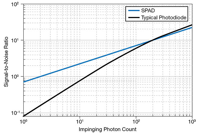
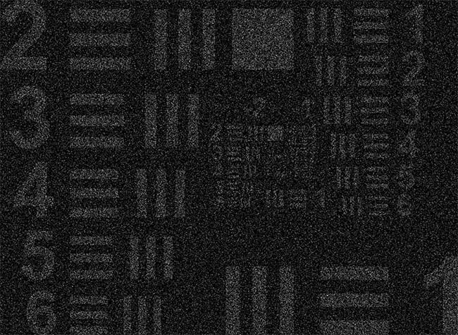
One additional application where SPAD technology is forging performance enhancements is high-speed imaging, in which image sensors typically suffer from low SNR. The shorter integration times in these operations lead to lower photon collection and pixel blur, while the faster readout speeds increase noise in the collected image. SPAD image sensors fully eliminate this noise to offer Poisson-maximized SNR.

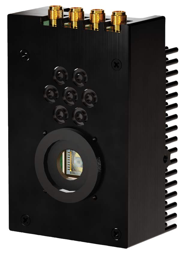
About Pi Imaging:
Pi Imaging Technology is fundamentally changing the way we detect light. We do that by creating photon-counting arrays with the highest sensitivity and lowest noise.
We enable our partners to introduce innovative products. The end-users of these products perform cutting-edge science, develop better products and services in life science and quantum information.
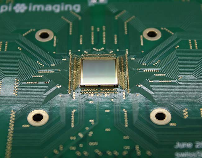
Pi Imaging Technology bases its technology on 7 years of dedicated work at TU Delft and EPFL and 6 patent applications. The core of it is a single-photon avalanche diode (SPAD) designed in standard semiconductor technology. This enables our photon-counting arrays to have an unlimited number of pixels and adaptable architectures.
Full article here: https://www.photonics.com/Articles/Single-Photon_Avalanche_Diodes_Sharpen_Spatial/p5/vo211/i1358/a67902
No comments:
Post a Comment
All comments are moderated to avoid spam and personal attacks.