A review article in Nature Communications by Wang et al. (Shanghai Institute of Technical Physics) discusses techniques for characterizing 2D photodetectors.
Full paper: https://www.nature.com/articles/s41467-023-37635-1
Abstract: Photodetectors based on two-dimensional (2D) materials have been the focus of intensive research and development over the past decade. However, a gap has long persisted between fundamental research and mature applications. One of the main reasons behind this gap has been the lack of a practical and unified approach for the characterization of their figures of merit, which should be compatible with the traditional performance evaluation system of photodetectors. This is essential to determine the degree of compatibility of laboratory prototypes with industrial technologies. Here we propose general guidelines for the characterization of the figures of merit of 2D photodetectors and analyze common situations when the specific detectivity, responsivity, dark current, and speed can be misestimated. Our guidelines should help improve the standardization and industrial compatibility of 2D photodetectors.Device effective area
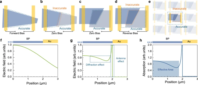
a Photoconductive photodetector. b Planar junction photodetector. c, d Vertical junction photodetectors with zero and reverse bias, respectively. e Focal plane photodetector. The dashed blue lines in a–e are suggested accurate effective areas. The dashed orange lines in b, d, and e are potential inaccurate effective areas for respective types. f Field intensity of the Gaussian beam with the beam waist w0 = 2.66 μm, here BP represents black phosphorus. g Wave optics simulation result of the electric field distribution at the upper surface of the device with plane wave injected. h Calculated absorption with the Gaussian beam with the beam waist w0 = 2.66 μm multiplying the wave optics simulation profile shown in (g).
Responsivity
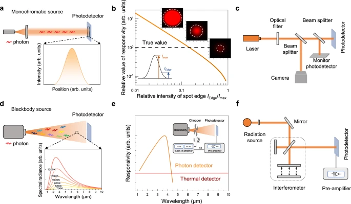
a Monochromatic laser source measurement system, where the laser spot intensity follows the Gaussian distribution. b Relative intensity of the edge of the spot under the researcher’s estimation. The inset shows three spots with the same beam waist and color limit, the only difference of which is the beam intensity. with different intensities and the same beam waist. The estimated radius of spot size shows vast differences. c Laser spot size and power calibration measurement system. d Photon composition of blackbody radiation source, and the radiation distribution in accordance with Planck’s law. e Typical response spectrum of photon detector and thermal detector. The inset shows a diagram of the blackbody measurement system. f Schematic diagram of FTIR measurement system.
Dark current
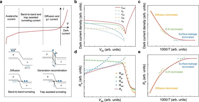
a Typical dark current mechanism, the dashed lines, filled and empty circles and arrows represent quasi-fermi level, electrons, holes, and carrier transport direction. b Characterization and analysis of dark current for UV-VIS photodetectors. The solid red line is the Id–V characteristic curve measured with a typical VIS photodetector. The green, dark blue, orange, and light blue dashed lines represent the fitted current components of generation-recombination, band-to-band tunneling, diffusion, and trap-assisted tunneling with analytic model. c Dominant dark current for typical photovoltaic photodetectors at different temperatures. d Characterization and analysis of dynamic resistance for infrared photodetectors. The solid red line is the Rd–V characteristic curve measured with a typical infrared photodetector. The orange, green, light blue, and dark blue dashed lines represent the fitted current components of diffusion, generation-recombination, trap-assisted tunneling, and band-to-band tunneling with analytic model. e Dynamic resistance of typical photovoltaic photodetectors at different temperatures.Other noise sources
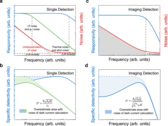
a Noise and responsivity characteristics for photodetectors with different response bandwidths for single detection (the blue line represents the typical responsivity curve of photodetectors of high response bandwidth, the green line represents the typical responsivity curve of photodetectors of low response bandwidth, and the red line represents the typical noise characteristics. The vertical dashed lines represent the −3 dB bandwidth for photodetectors with high and low response bandwidth). b Overestimation of specific detectivity based on noise characteristics for single detection. The solid and dashed lines present the calculated specific detectivity with D∗=RAdΔfin from the measured noise and estimated noise of thermal noise and shot noise (ignoring the 1/f noise and g-r noise). c Noise and responsivity characteristics for photodetectors of imaging detection. d Overestimation of specific detectivity based on noise characteristics for imaging detection. The solid and dashed lines present the calculated specific detectivity with D∗=RAdfB∫0fBindf from the measured noise and estimated noise of thermal noise and shot noise (ignoring the 1/f noise and g-r noise).
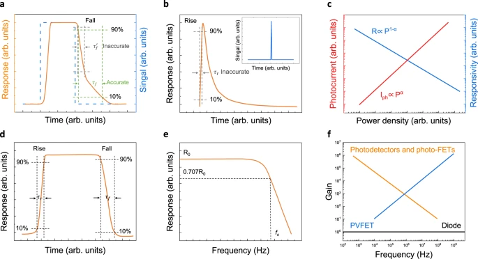
Time parameters
a Calculated fall time does not reach a stable value which is inaccurate, where τf′ is inaccurate calculated fall time, τf is accurate calculated fall time. (The bule line represents the square signal curve, the yellow line represents the typical response curve of 2D photodetectors.) b Response time measurement of photodetector may not reach a stable value under pulse signal, which will lead to an inaccurate result. The inset shows pulse signal. The τr is inaccurate calculated rise time. c Variation of photocurrent and responsivity of photoconductive photodetectors with the incident optical power density14. d Rise and fall response time of photodetector should be calculated from a complete periodic signal. e Typical −3 dB bandwidth response curve of photodetector, where R0 represents stable responsivity value, fc represents the −3 dB cutoff frequency. f Gain-bandwidth product of various photodetectors, where photo-FET is photo-field-effect transistor, PVFET is photovoltage field-effect transistor14.
for a reversely bias photodiode, we talk often diffusion current as one component of dark current. But in reality, this should be the drift current. Since the reverse bias voltage increases the electric field in the PN junction and reduces the diffusion current and the dak current is formed essentially of minority drift current. Why we talk always "diffusion current" here? Any one can give an explanation please? Thanks!
ReplyDeleteThe current, constant in x in steady state, is always a combination of diffusion and drift, and the relative proportions depends on which region you look at. You are right, in the depletion region, the current is almost entirely drift current. But if you move to the edge of the depletion region, where the electric field nearly vanishes, the current is mostly diffusion current. The diffusion of carriers from deeper in the neutral region (field-free region) limits the total current. Essentially the current is supply limited from the diffusion process. Because of this, we refer to the total dark current as diffusion current. Actually, there is also thermal (or optical) generation in the neutral region and the depletion region. This adds to the reverse current (with optical generation it is not dark current, of course). In theory the reverse (dark) current saturates with reverse voltage due to diffusion limitation, even the depletion field continues to get stronger. In most devices, the reverse current continues to increase with reverse bias due to thermal generation in the vicinity of the junction,
DeleteThanks so much Eric!
DeleteOne thing in this topic that is always a bit confusing to me are the magnitudes. There are many different reasons for non ideal behaviour of a CIS, "noise". I was browsing through Alberts blog recently and found one interesting sentence here: https://harvestimaging.com/blog/?p=1028: "Once there is light shining on the sensor and once the sensor is delivering enough signal, the photon shot noise will be the largest noise component and the measurement results will be dominated by this photon shot noise .".
ReplyDeleteIn one application on my desk I have a sensor with quite small useable FW, lets say about 4ke-, so in the 12bit output 1 electron contributes to 1 digital in the output. Exposure time in the few ms range, global shutter. When I grab a homogenous scene (integrating sphere) hundreds of times at a constant illumination that leads to a mean grey value of lets say 3000 (at the 12bit output number) and look for the variation in the grey value (always at the same pixel across the hundreds frames) I see a magnitude of variation of more than 300 with a std deviaiton of maybe 70 (i know no std distribution here, but just for the magnitude...). I also notice that this value virtually does not change with temperature change. So 20 degress more or less result in more or less exactly the same variation of grey values.
Do I read the quote of Alberts post above correctly? Is the main reason for this behaviour photon shot noise? is a magnitude of 10% of the signal output a reasonable number?
If were talking about a single pixel exposed to a temporally stable light source then there are really two main contributions of noise: read noise and shot noise (photon noise). Shot noise increases with the square root of the number of photons observed by the pixel per-integration time, whereas read noise is mostly signal independent (constant). No light means no shot noise. So as you increase the number of photons interacting with the pixel (i.e. increase the impinging light intensity) the total noise of the pixel transitions from being dominated by read noise to being dominated by shot noise. Jim Janesick's book "Photon Transfer" does a great job of explaining this. Chapter 5 may be of help to you.
Delete3000 electron's photon shot noise is 55 electrons. 70 looks good match.
Deleteso for an estimation... we can say that "the square root of the number of electrons of the singal give the magnitude of the standard deviation of shot noise", as simple as that?
Deletejust an addon... it really seems to be as simple as that. at https://en.wikipedia.org/wiki/Shot_noise you have the quote: "the standard deviation of shot noise is equal to the square root of the average number of events". So if you have for example a signal of 3000e-, meaning a grey value of 3000 (in 12bit output), the standard deviation of shot noise in this is about 55 grey values. We run a few tests also on temperature dependence of this and how the stddev reacts on variation of other parameters. It seems in our setup (enough light to have exposure time in the low ms for example), this is the dominant source of 'noise' and alberts quote "Once there is light shining on the sensor and once the sensor is delivering enough signal, the photon shot noise will be the largest noise component and the measurement results will be dominated by this photon shot noise .". is important for us. It is also a surprise to see that it really seems to be as simple as that - square root of number of electrons. Other effects like temperature (it virtually does not matter if we run the camera at 30 or 50deg) seem to be insignificant.
Deleteand addon#2... it is fascinating how exact the numbers match the theory. we tested 3 sensors on the integrating sphere, one with fullwell 6.5ke-, one with 10.5k and one with 140k. We measured the temporal noise of each pixel across many frames at 200DN mean (in the 8bit grey value, so about 80% of the full signal). You expect to get sqrt(0.8xfullwell) electrons as standard deviation and we get exactly this number in the measurment, 3.6DN (in the 8bit domain) for the 6.5k FW, 2.3DN for 10.5k and 0.7 for the 140ke- sensor.
ReplyDeleteFor industrial global shutter use cases (you tend to have short exposure times and rather high ammount of light), this seems to be the single relevant factor for noise in images i guess. it does not matter if you run such a industrial camera at 20 or 60deg for example, this temporal noise figures virtually do not change. I dont know why the datasheets of such cameras and image sensors are filled with information about effects that are irrelevant besides this single formula (that is never mentioned ;-): stdev of shot noise = sqrt(signal)
Read noise is important as it is a dominant noise when there is little photons i.e. for low light scenes. And since it is temperature dependent, at higher sensor temperatures it makes low light sensitivity worse.
Deletebut where in industrial cameras do you have this? I mean the typical application of the typical industrial global shutter sensors like the Sony Pregius, Gpixel Gmax ish type of devices. Cameras on robots that grab a scene for a robot to decide for a move to the left or to the right. You have rather powerful external illumination, rather short (low ms) exposure time. I would guess this is the 90% problem of this type of image sensors. The limit in terms of temporal noise in such applications - limiting the accuracy of position measurement in a scene is purely shot noise. I dont know why this effect is never mentioned. You have numbers like this read noise in the datasheet but i guess in 90% of the applications of this sensors it is irrelevant.
DeleteWhenever there is throughput to be considered--think of inspection. You do have a bright source, but you would like to take advantage of it by reducing the integration time. There goes your shot-noise limited operation :)
DeleteSure, if you have enough light even for a short exposure time you will not be read noise limited, and all the noise you see is the photon shot noise. The datasheets are not including shot noise as when this much light is available the SNR is rather high and not limiting any vision related applications.
Delete> but you would like to take advantage of
ReplyDelete>it by reducing the integration time.
> There goes your shot-noise limited operation :)
well - not at all, or what do I not understand? the square root of the ammount of photons/electrons that build your signal defines your shot noise limit. No matter how long your integration time is you have this effect. Only if you have very long integration time other effects kick in and start to dominate on top of shot noise. The shot noise limit that will always be there, right? If your average signal comes from 900 electrons, the stddev of shot noise will be 30 electrons - no matter how long you expose. If you expose 1ms to reach this signal, all other effects will be irrelevant compared to the 30electrons shot noise.
The shot noise limit refers to the best possible signal to noise ratio a pixel can achieve, which is physically limited by photon shot noise. Real cameras have other sources of noise, e.g. read noise, so the way you get close to this shot noise limit is by getting more light on your pixels and thus increasing your shot noise (higher incident illumination or a longer integration time will achieve this). If you increase shot noise enough the total noise of your pixel eventually becomes *nearly* completely comprised of shot noise and you enter the "shot noised limited" region of the pixel's dynamic range. Some of these new deep sub-electron read noise sensors have very little read noise and can reach shot noise limited imaging at much lower incident illumination compared to traditional CMOS and CCD sensors. This is what makes them great for low-light imaging.
Delete@Aaron, correct, but also don't forget spatial noise. For applications such as inspection, you also need to be above spatial noise as well. It is true that we have image sensors that have sub electron read noise, but it is achieved only at high gain settings ( limiting full well) and highest ADC resolution to minimize quantization noise. Plus, these very low-noise image sensors may not meet other optical requirements. When throughput is being pushed, having "more than enough" photons on the sensor is never going to happen, as customers try to push it to the limits till other things break down (such as object recognition or contour detection algorithms)
DeleteThanks Aaron. The limit is calculated based on the number of electrons - or photons? could this be my misunderstanding? (i still dont understand why i measure the theoretical limit and the other sources of noise seem to be irrelevant ;-)
DeleteI run the test on the integrating sphere with the 10500e fullwell sensor with lowest gain (so I assume I see about the 10500e at a pixel with 255DN...). mean greyvalue 80% of saturation, so a mean of 8400e form the signal. Theoretical limit for shot noise stdev: sqrt(8400)=91. 91/10500*256=2.23DN, right? I take 200 frames and for each of 1000x1000 pixels calculate the standarddeviation and make a histogram of these. The measured mean value of this 1M stdev over 200 frames is 2.3DN. Is this coincidence?
The sensor has a QE of ~60% at the used wavelength, so the base signal for 10500e is about 17500 photons, right? do I need to think of sqrt(17500*0.8)=118, which scales to 118/17500*256=1.7DN then?
So just to understand the magnitude... do I see 1.7DN 'physical limit' and on top of this 0.6DN caused by other sources of temporal noise? Or do I really see a physical limit of 2.3DN and also measure this and the other sources of noise are irrelevant for my set of parameters (rather strong illumination=short exposure time of few ms)?
True. Once you starting talking about arrays of pixels then you have to consider FPN as well. There is a lot more that could be said to describe the performance of actual sensors. I also chose not to mention dark shot noise and dark FPN but that could be discussed too.
DeleteDid you also check the noise histogram in the dark?
DeleteThe noise is in terms of electrons as the full well is characterized in electrons. You can then calculate back how more it is in photons.
ReplyDeleteThis calculation is for a temporal noise, if you want to compute the total noise you may calculate standard deviation of the 100s of pixels ROI that corresponds to uniformly lit surface. This deviation represents all noise sources - temporal (read, shot, dark current, etc.) and FPN (row, column) and is relevant at all light levels, even dark. You don't need to average over multiple frames as the temporal variation will be included already between pixels of the ROI from a single image.
Thanks for your answers! really interesting to play with parameters and learn about this topic. You know what happened when we use a laser instead of a LED to illuminate the integrating sphere? The temporal noise "freezes" - so it becomes more or less a static noise like FPN with very little temporal variation, similar standard deviation - not from frame to frame but laterally. It is a fascinating effect, if you have a slight vibration on the optical table it looks "like a liquid", and once it is silent it "freezes". Did anyone of you try this before? What is the explaination for such an effect?
ReplyDeleteProbably because you are using a coherent source?
Deletethe probability of a photon to generate a electron during exposure is 50% if QE is 50%, right? so if the selected illumination results in a mean of 3000electrons it is like throwing a coin 6000 times - in the mean of millions pixels you get 3000, but not on the single pixel. Isnt this what shot noise is about? throwing a coin 6000 times does not give you 3000 times the same side - it gives you a mean of 3000 with a stddev of sqrt(6000). The pixel itself does not know anything about the nature of the light source but integrates photons/electrons during exposure. How is it possible that the temporal noise is so different if the integrating sphere is illuminated with a laser?
DeleteI think you may be confusing QE which is a property of the material and design, with photon shot noise which originates at the source?
DeleteYou may have more light when you use laser so for high number of electrons you have a good signal to noise ratio. With more light the column FPN may be pronounced, especially if it is not corrected for. And thus visually you cannot notice temporal noise, only a more pronounced static one - FPN.
DeleteThe explanation of the slow movements in the image with vibrations is that you are probably seeing rolling shutter effects that would disappear if you used a global shutter camera.
Agreed with the comment above. The freezing noise spots you observed were speckles, from cohere light source.
DeleteRegarding "..confusing QE...with photon shot noise..." Actually both these things matter when it comes to shot noise. A hypothetical noise-less stream of photons going through absorption will lead to noise in the the number of photoelectrons generated, with a mean (which leads to the QE number) and a variance. An incoming stream of photons described by the Poisson statistics, will lead to a "stream" of photoelectrons that also follow Poisson statistics, where the mean is determined by the photon stream mean and the mean quantum efficiency. The SNR of the photoelectrons will be reduced compared to that of the photon stream. Similarly, photons going through the atmosphere and other materials on the way to silicon are scattered and/or absorbed in a statistical process which also leads to Poisson statistics. It is pretty interesting all in all. All of this assumes that there are enough events for a hypothetical noiseless stream of photons to be attenuated and randomized into a stream that follows Poisson statistics. A reference for all this can be found in Saleh and Teich. (found here, for example: https://www.amazon.com/Fundamentals-Photonics-Wiley-Applied-Optics/dp/1119506875/ref=d_pd_sbs_sccl_2_1/139-9162369-8266356
DeleteHi, and thanks for your comments and your help in understanding this. We already ordered the 'fundamentals of photonics' book (thanks for the hint Eric and also for your comment).
ReplyDeletewe need to make a few more measurements in order to quantify the effect for example with the laser illuminated integrating sphere.
we use 3 global shutter sensors as test objects here. so no rolling shutter artifacts.
also FPN is not the topic of this experiment (it is important of course, but just for this topic the aim is to understand what contributes to temporal noise, and we use 3 different image sensors to get some measurement data and how things change if parameters are changed...)
I think one point we learned is that the lower limit of temporal noise is shot noise - since the measurement in the pixel is based on a limited number of events. Even if all other noise sources were removed, sqrt(nr of events) will always be the lower limit of temporal noise.
impresive
ReplyDelete