Wednesday, August 30, 2023

LiDAR miniaturization

The April 2023 edition of ADAS and Autonomous Vehicles International features a cover story article by Dr. Sabbir Rangwala on miniaturization of LiDAR sensors.

https://www.ukimediaevents.com/publication/9cb6eeeb/36


Obstacles to lidar miniaturization

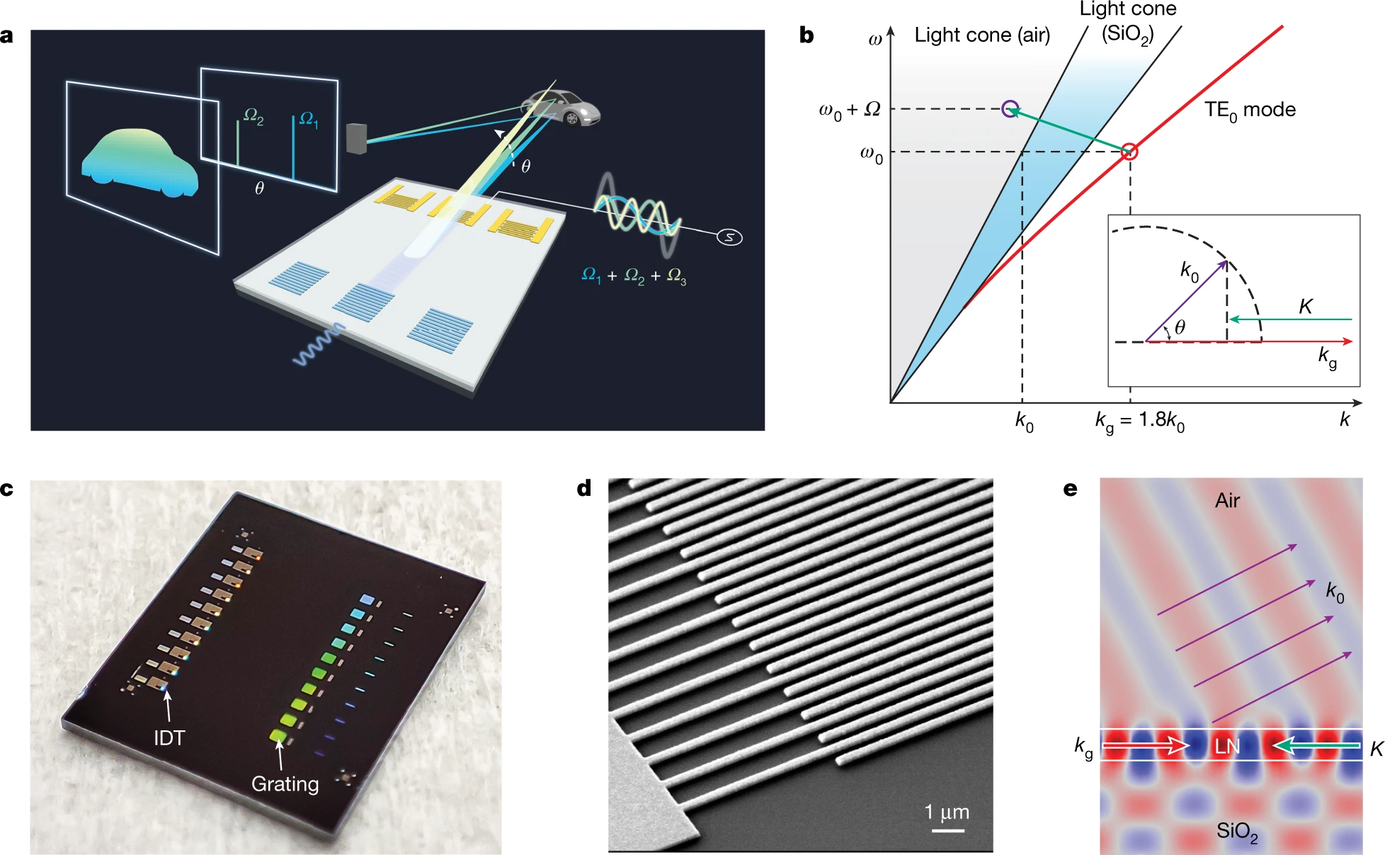
The single biggest obstacle to lidar miniaturization is the laser. Producing photons from electrons is difficult and inefficient. The telecommunication revolution of the 1990s went a long way to progress semiconductor lasers from research labs to the factory and into terrestrial and undersea fiber-optic networks. Lidar poses challenges of a different nature, as it involves laser energy transmission in free space. The transmit-receive process is inefficient due to atmospheric attenuation and range-related optical coupling losses. Addressing thousands of image elements over a reasonable FoV with acceptable resolution and high frame rates requires power levels that are difficult to realize from semiconductor lasers. This leads to the use of optical amplification (fiber lasers), large laser arrays (like VCSELs) or time and space sharing of the laser energy (scanning). Eye safety is another consideration. The 800-900nm wavelengths used by some lidars have low eye-safety margins. This improves with 1,300-1,500nm lasers, but there are still limits to the amount of safe power density that can be used to achieve a certain level of performance. Bulky system packaging and optics are required to engineer eye-safe solutions. Lasers are inefficient and sensitive to temperature. Roughly 70-80% of the electrical energy used is converted to heat (which needs to be managed). Automotive temperature ranges also cause problems because of wavelength shifts and further efficiency degradation. The complex III-V semiconductors used for lasers (GaAs or InGaAs) degrade faster at higher temperatures and in the presence of moisture. Active cooling and more complex packaging are required. At a system level, lidar currently requires hybrid integration of different materials: complex III-V semiconductors, silicon processing electronics, glass fibers, bulk optics (focusing lenses, isolators), scanning mechanisms, thermal management and complex packaging.

Current approaches
The FoV is addressed with purely solid-state approaches (no moving parts): using a single laser pulse or flash, in which all image pixels are simultaneously addressed (PreAct, TriEye, Ouster); or electronic scanning arrays of monolithic silicon SPADs and GaAs VCSELs that address regions in the FoV sequentially (Opsys, Hesai). The VCSEL-SPAD approach leverages thedevelopments, productization and integration of ToF (time-of-flight) lidar in smartphones at 905/940nm wavelengths (exact values vary and are proprietary); or optical scanning using a combination of phase-tuning antennas (optical phase arrays or OPAs) and wavelength dispersion, implemented in chip-scale silicon photonics platforms (Analog Photonics). This platform is compatible with FMCW-coherent lidar, which simultaneously measures range and radial velocity and operates in the 1,500nm wavelength band. PreAct focuses on short-range lidar for in-cabin sensing and road-facing applications. The approach is disruptive – it uses low-cost, off-the-shelf, CCD arrays and LED (versus laser) light sources to create 3D images based on indirect time of flight (iToF, like in gaming applications). The TrueSense T30 operates at an impressively high 150Hz frame rate, which is important for fast reaction times associated with short-range applications like blind spot obstacle avoidance and pedestrian safety. The size envelope includes an 8MP RGB camera and electronics that fuse the visible and 3D images. Eliminating the RGB sensor can reduce the size further. TriEye’s SEDAR (Spectrum Enhanced Detection and Ranging) is a flash lidar that uses a 1.3Mp CMOS-based germanium-silicon SWIR detector array and an internally developed, Q-switched, high peak-power, solid-state pumped diode laser that flashes the entire FoV. The higher wavelength provides greater eye-safety margins, which enables the use of higher laser power. Opsys uses a unique implementation of electronically addressable high-power VCSEL and SPAD arrays to achieve a solid-state lidar with no moving parts. It operates over automotive temperature ranges without requiring any type of active cooling or temperature stabilization. Hesai is in production for multiple automotive customers with the AT128 long-range lidar (which uses mechanical scanning for the HFoV). The FT120 is a fully solid-state lidar that uses electronic scanning of the VCSEL and SPAD arrays and is targeted for short-range applications (blind spot detection, in-cabin, etc). The company went public in January 2023, and is currently in a quiet period.

Tuesday, August 29, 2023

Imec thin-film pinned photodiode for SWIR sensing in Nature Electronics

Press release: https://www.imec-int.com/en/press/imec-integrates-thin-film-pinned-photodiode-superior-short-wave-infrared-imaging-sensors

Imec integrates thin-film pinned photodiode into superior short-wave-infrared imaging sensors

LEUVEN (Belgium), 14 August, 2023—Imec, a world-leading research and innovation hub in nanoelectronics and digital technologies, presents the successful integration of a pinned photodiode structure in thin-film image sensors. With the addition of a pinned-photogate and a transfer gate, the superior absorption qualities of thin-film imagers -beyond one µm wavelength- can finally be exploited, unlocking the potential of sensing light beyond the visible in a cost-efficient way.

Detecting wavelengths beyond visible light, for instance infrared light, offers clear advantages. Applications include cameras in autonomous vehicles to ‘see’ through smoke or fog and cameras to unlock your smartphone via face recognition. Whilst visible light can be detected via silicon-based imagers, other semiconductors are necessary for longer wavelengths, such as short-wave infrared (SWIR).

Use of III-V materials can overcome this detection limitation. However, manufacturing these absorbers is expensive, limiting their use. In contrast, sensors using thin-film absorbers (such as quantum dots) have recently emerged as a promising alternative. They have superior absorption characteristics and potential for integration with conventional (CMOS) readout circuits. Nonetheless, such infrared sensors have an inferior noise performance, which leads to poorer image quality.

Already in the 1980’s, the pinned photodiode (PPD) structure was introduced for silicon-CMOS image sensors. This structure introduces an additional transistor gate and a special photodetector structure, by which the charges can be completely drained before integration begins (allowing reset operation without kTC noise nor the effect of the previous frame). Consequently, because of lower noise and improved power performance, PPDs dominate the consumer market for silicon-based image sensors. Beyond silicon imaging, incorporating this structure was not possible up until now because of the difficulty of hybridizing two different semiconductor systems.

Now, imec demonstrates successful incorporation of a PPD structure in the readout circuit of thin-film-based image sensors; the first of its kind. A SWIR quantum-dot photodetector was monolithically hybridized with an indium-gallium-zinc oxide (IGZO)-based thin-film transistor into a PPD pixel. This array was subsequently processed on a CMOS readout circuit to form a superior thin-film SWIR image sensor. “The prototype 4T image sensor showed a remarkable low read-out noise of 6.1e-, compared to >100e- for the conventional 3T sensor, demonstrating its superior noise performance” stated Nikolas Papadopoulos, project leader ‘Thin-Film Pinned Photodiode’ at imec. As a result, infrared images can be captured with less noise, distortion or interference, and more accuracy and detail.

Pawel Malinowski, imec Program Manager ‘Pixel Innovations’ adds: “At imec, we are at the forefront of bridging the worlds of infrared and imagers, thanks to our combined expertise in thin-film photodiodes, IGZO, image sensors and thin-film transistors. By achieving this milestone, we surpassed current pixel architectural limitations and demonstrated a way to combine the best performing quantum-dot SWIR pixel with affordable manufacturing. Future steps include optimization of this technology in diverse types of thin-film photodiodes, as well as broadening its application in sensors beyond silicon imaging. We are looking forward to further these innovations in collaborations with industry partners.”

The findings are published in the August 2023 edition of Nature Electronics "Thin-film image sensors with a pinned photodiode structure". Initial results were presented at the 2023 edition of the International Image Sensors Workshop.

J. Lee et al. Thin-film image sensors with a pinned photodiode structure, Nature Electronics 2023.
Link (paywalled): https://www.nature.com/articles/s41928-023-01016-9

Abstract
Image sensors made using silicon complementary metal–oxide–semiconductor technology can be found in numerous electronic devices and typically rely on pinned photodiode structures. Photodiodes based on thin films can have a high absorption coefficient and a wider wavelength range than silicon devices. However, their use in image sensors has been limited by high kTC noise, dark current and image lag. Here we show that thin-film-based image sensors with a pinned photodiode structure can have comparable noise performance to a silicon pinned photodiode pixel. We integrate either a visible-to-near-infrared organic photodiode or a short-wave infrared colloidal quantum dot photodiode with a thin-film transistor and silicon readout circuitry. The thin-film pinned photodiode structures exhibit low kTC noise, suppressed dark current, high full-well capacity and high electron-to-voltage conversion gain, as well as preserving the benefits of the thin-film materials. An image sensor based on the organic absorber has a quantum efficiency of 54% at 940 nm and read noise of 6.1e–.


Monday, August 28, 2023

Paper on NIR quantum dot sensor

Xu et al published a paper titled "Near-Infrared CMOS Image Sensors Enabled by Colloidal Quantum Dot-Silicon Heterojunction" in MDPI Electronics.

Link: https://www.mdpi.com/2079-9292/12/12/2695

Abstract:  The solution processibility of colloidal quantum dots (CQDs) promises a straightforward integration with Si readout integrated circuits (Si-ROICs), which enables a near-infrared (NIR) CMOS image sensor (CIS; CMOS stands for complementary metal-oxide semiconductor). Previously demonstrated CQD NIR CISs were achieved through integrating CQD photodiode or PhotoFET with Si-ROCIs. Here, we conduct a simulation study to investigate the feasibility of a NIR CIS enabled by another integration strategy, that is, by forming a CQD-Si heterojunction. Simulation results clearly show that each active pixel made of CQD-Si heterojunction photodiode on the CIS sensitively responds to NIR light, and generated photocarriers induce changes in electrostatic potentials in the active pixel. The potential changes are read out through the integrated circuits as validated by the readout timing sequence simulation.


Schematics of an active pixel of a CQD-based NIR CIS.


 (a) I-V curves of NiO/CQD/Si heterojunction photodiode in the dark and various light intensities. (b) Photocurrent at various intensities. (c) Responsivity values as a function of intensity showing good linearity.
 
 
Electrostatic potential of the active pixel along the horizontal red dashed line in Figure 1 (y = 10 nm) in (a) dark and (b) under illumination. Light intensity is 13 W/cm2.


Timing sequence diagram of the active pixel (a) in the dark and (b) under illumination.


Friday, August 25, 2023

Acousto-optic beam steering for LiDARs

Li et al from U. Washington in Seattle published a paper titled "Frequency–angular resolving LiDAR using chip-scale acousto-optic beam steering"

Link: https://www.nature.com/articles/s41586-023-06201-6

Abstract:
Thanks to its superior imaging resolution and range, light detection and ranging (LiDAR) is fast becoming an indispensable optical perception technology for intelligent automation systems including autonomous vehicles and robotics. The development of next-generation LiDAR systems critically needs a non-mechanical beam-steering system that scans the laser beam in space. Various beam-steering technologies have been developed, including optical phased array, spatial light modulation, focal plane switch array, dispersive frequency comb and spectro-temporal modulation. However, many of these systems continue to be bulky, fragile and expensive. Here we report an on-chip, acousto-optic beam-steering technique that uses only a single gigahertz acoustic transducer to steer light beams into free space. Exploiting the physics of Brillouin scattering, in which beams steered at different angles are labelled with unique frequency shifts, this technique uses a single coherent receiver to resolve the angular position of an object in the frequency domain, and enables frequency–angular resolving LiDAR. We demonstrate a simple device construction, control system for beam steering and frequency domain detection scheme. The system achieves frequency-modulated continuous-wave ranging with an 18° field of view, 0.12° angular resolution and a ranging distance up to 115 m. The demonstration can be scaled up to an array realizing miniature, low-cost frequency–angular resolving LiDAR imaging systems with a wide two-dimensional field of view. This development represents a step towards the widespread use of LiDAR in automation, navigation and robotics. 


a, Schematic illustration of the FAR LiDAR scheme based on AOBS. b, Dispersion diagram of the acousto-optic Brillouin scattering process. The dispersion curve of the TE0 mode of the LN planar waveguide is simulated and plotted as the red curve. At frequency ω0 (wavelength 1.55 μm), the mode wavenumber is 1.8k0 (red circle). The counter-propagating acoustic wave (green arrow) scatters the light into the light cone of air (purple circle in the grey shaded area). For clarity, the frequency axis is not to the scale. Inset: momentum vector relation of the Brillion scattering. The light is scattered into space at an angle θ from the surface. c, Photograph of an LNOI chip with ten AOBS devices. d, Scanning electron microscope image of the IDT. The period is chirped from 1.45 to 1.75 μm. e, Finite-element simulation of the AOBS process showing that light is scattered into space at 30° from the surface.

a, Superimposed image of the focal plane when the beam is scanned across a FOV from 22° to 40°, showing 66 well-resolved spots. b, Magnified image of one spot at 38.8°. The beam angular divergence along kx is 0.11° (bottom inset) and along ky is 1.6° (left inset), owing to the rectangular AOBS aperture. c, Real-space image of light scattering from the AOBS aperture. The light intensity decays exponentially from the front of the IDT (x = 0), owing to the propagation loss of the acoustic wave. Fitting the integrated intensity along the x axis (bottom inset, yellow line) gives an acoustic propagation length of 0.6 ± 0.1 mm. d, The measured frequency–angle relation when the beam is steered by sweeping the acoustic frequency. a.u., arbitrary units. e–h, Dynamic multi-beam generation and arbitrary programming of 16 beams (e) at odd (f) and even (g) sites, and in a sequence of the American Standard Code for Information Interchange code of characters ‘WA’ (h).


a, Schematics of the FAR LiDAR system. The transmitter includes a fixed-wavelength, fibre-coupled laser source, an EOM for FMCW (used in Fig. 4) and an AOBS device driven by a radio frequency source to steer the beam. An additional mirror is used to deflect the light towards the object. The coherent receiver uses homodyne detection to resolve the frequency shift of the reflected light by beating it with the LO, which is tapped from the laser source. A BPD is used to measure the beating signal, which is sampled by a digital data acquisition (DAQ) system or analysed by a real-time spectrum analyser. As a demonstration, a 60 × 50 mm cutout of a husky dog image made of retroreflective film is used as the object. It is placed 1.8 metres from the LiDAR system. b, Spectra of the beating signal at the receiver when the AOBS scans beam across the FOV. Using the measured frequency–angle relation in Fig. 2d, the beating frequency can be transformed to the angle of the object. c, FAR LiDAR image of the object. The position and brightness of each pixel are resolved from the beating frequency and power of the signal, respectively. d,e, The raw beating signal of two representative pixels (orange, d; purple, e).


a, Time–frequency map of the transmitted light (bottom, Tx) and received light (top, Rx), both are chirped by a triangular waveform. The chirping rate is g = 1 MHz μs−1. The frequency of the received light is upshifted by the acoustic frequency Ω/2π (RBW, resolution bandwidth). a.u., arbitrary units. b, Top, schematic illustration of the frequency of the FMCW signal as a function of time. The frequency alternates between Ω/2π ± fB. Bottom, measured time–frequency map of the FMCW signal. Because of the upper sideband and the lower sideband) generated by the EOM, the FMCW frequencies at Ω/2π ± fB are present all the time. Also present is the frequency component at Ω/2π, which is from the unsuppressed optical carrier and used for FAR imaging. c, Spectra of FMCW signals when different acoustic frequencies (red, 1.6 GHz; green, 1.7 GHz; purple, 1.8 GHz) are used to steer the beam to reflectors placed at different angles and distances. d, 3D LiDAR image of a stainless steel bolt and a nut, placed 8.0 cm apart from each other, acquired by combining FAR and FMCW schemes. The FMCW chirping rate is g = 1 MHz μs−1 and frequency excursion fE = 1 GHz. Inset: photograph of the bolt and nut as the imaging objects. e, FMCW spectra of two representative points (A and B) in d, showing signals at Ω/2π (offset to zero frequency) and Ω/2π ± fB (offset to ±fB). f, Zoomed-in view of the FMCW signals at fB for point A and B. g, Our vision of a monolithic, multi-element AOBS system for 2D scanning, which, with a coherent receiver array (not shown), can realize 2D LiDAR imaging.


Wednesday, August 23, 2023

Videos du jour [Aug 23, 2023]


Snappy Wide 8K wide aspect ratio CMOS image sensor

Snappy Wide is Teledyne e2v's new 8K wide aspect ratio CMOS image sensor designed specifically for logistics applications where larger conveyor belts are becoming increasingly common. A single Snappy Wide sensor can cover this large field of view successfully, replacing multiple sensors for a more efficient and cost-effective solution.


Recurrent Vision Transformers for Object Detection with Event Cameras (CVPR 2023)

We present Recurrent Vision Transformers (RVTs), a novel backbone for object detection with event cameras. Event cameras provide visual information with sub-millisecond latency at a high-dynamic range and with strong robustness against motion blur. These unique properties offer great potential for low-latency object detection and tracking in time-critical scenarios. Prior work in event-based vision has achieved outstanding detection performance but at the cost of substantial inference time, typically beyond 40 milliseconds. By revisiting the high-level design of recurrent vision backbones, we reduce inference time by a factor of 6 while retaining similar performance. To achieve this, we explore a multi-stage design that utilizes three key concepts in each stage: First, a convolutional prior that can be regarded as a conditional positional embedding. Second, local and dilated global self-attention for spatial feature interaction. Third, recurrent temporal feature aggregation to minimize latency while retaining temporal information. RVTs can be trained from scratch to reach state-of-the-art performance on event-based object detection - achieving an mAP of 47.2% on the Gen1 automotive dataset. At the same time, RVTs offer fast inference (less than 12 ms on a T4 GPU) and favorable parameter efficiency (5 times fewer than prior art). Our study brings new insights into effective design choices that can be fruitful for research beyond event-based vision.
Reference:
M. Gehrig, D. Scaramuzza
"Recurrent Vision Transformers for Object Detection with Event Cameras"
IEEE Conference on Computer Vision and Pattern Recognition (CVPR), Vancouver, 2023
PDF: https://arxiv.org/abs/2212.05598
Code: https://github.com/uzh-rpg/RVT


Market news: CIS market predictions, Sony Q1-2023 results

In recent Medium blog posts Ming-Chi Kuo offers some predictions for CIS market in 3Q23 and beyond.

I. Industry background and current situation:
 The wide camera CIS of the two iPhone 15 standard models will be upgraded to 48MP and adopt a new stacked CIS design. Due to the low yield rate, Sony has increased the CIS production capacity for Apple by 100–120% to meet Apple’s demand, resulting in a significant reduction in high-end CIS supply for Android.
 The global CIS wafer reconstruction (RW) key supplier Tong Hsing’s earnings call pointed out that the bottom of the CIS industry is 3Q23.
 China’s semiconductor industry policy continues to implement the domestic replacement strategy, which is the main reason why Tong Hsing is conservative in its future mobile phone CIS RW business (orders continue to be lost to Chinese competitors).
 The current inventory in the CIS supply chain has improved to a normal level (10–14 weeks) from 30–40 weeks in 1H23.
 AI visualization applications will be the other key to driving CIS growth in the long term. The most visible application at this stage is self-driving cars, and the next most likely is robotics.

II. Will Semi will benefit from a significant market share gain of high-end CIS in the next few years:
 As Sony has reduced the supply of high-end Android CIS, brand vendors need to actively seek alternative solutions, benefiting Will Semi’s high-end CIS (64MP+) order growth (since 2H23). Will Semi’s high-end CIS market share is expected to increase significantly from 3–5% in 2023 to 10–15% and 20–25% in 2024 and 2025, respectively, which is conducive to long-term revenue and profit growth.
 The current inventory level of Will Semi has improved to a normal level (about 12 weeks).

III. The high-end CIS cooperation between Smartsens and Chinese brands will become closer:
Given that more and more of Sony’s capacity and R&D resources will continue to be consumed by Apple, Chinese brands such as Huawei will actively partner with more CIS suppliers, and in addition to Will Semi, Smartsens is a potential key supplier worthy of attention.


----------------


1. Following two 2H23 iPhone 15 standard models, two 2H24 iPhone 16 Pro models will also adopt stacked-designed CIS, so Sony’s high-end CIS capacity will continue to be tight in 2024, benefinting Will Semi to continue to obtain more orders for high-end CIS from Chinese smartphone brands (design- in & design-win).

2. Will Semi’s CIS shipments declined YoY in 1H23 due to inventory corrections, but due to inventory restocking and market share gains, the company will bottom out ahead of smartphone (end device) and resume growth from 2H23. Will Semi CIS shipments will improve significantly in 2023, growing by about 8% YoY (vs. a decline of about 40% YoY in 2022), which is better than smartphones and most components.

3. As Sony’s high-end CIS capacity remains tight, Will Semi’s high-end CIS (48MP+) market share will continue to grow rapidly. It is expected that 2H23 high-end CIS shipments will increase by about 50% HoH to 36 million units, and shipments in 3Q23 and 4Q23 will be about 16 million and 20 million units, respectively. Benefiting from the significant increase in orders in 2H23, Will Semi’s high-end CIS shipments in 2023 will grow by about 35% YoY.

4. Among Will Semi’s high-end CIS, the main contributions come from OV50A, OV50E, OV50H and OV64B. The above mentioned CIS replaced many orders from Sony.
Looking forward to 2024, thanks to the tight capacity of Sony’s high-end CIS, Will Semi’s total CIS and high-end CIS shipments are expected to grow by about 15–20% YoY and 40–50% YoY, respectively. With the continued improvement in total shipments and product mix, sales and profit are expected to grow significantly from 2H23.


----------------

In other market news, Sony reported a 41% drop in operating income for the image sensor business. 

https://www.sony.com/en/SonyInfo/IR/library/presen/er/pdf/23q1_sonypre.pdf


Monday, August 21, 2023

Canon starts selling SPAD security camera

Link: https://www.usa.canon.com/shop/p/ms-500?cjevent=a2aac72b313b11ee83f885190a82b832&cjdata=MXxOfDB8WXww

MS-500

  •  Long-range ultra-high-sensitivity low-light camera
  •  Features the Canon-designed and developed 1-inch Single-Photon Avalanche Diode (SPAD) Sensor with approx. 3.2 million pixels
  •  B4 mount that supports Canon’s lineup of ultra-telephoto 2/3-inch broadcast zoom lenses
  •  The CrispImg2 Custom Picture Preset optimizes resolution and contrast while suppressing image noise
  •  Custom Picture Mode allows users to create up to 20 customized image quality settings for various shooting conditions
  •  Haze Compensation and Smart Shade Control features reduce the effects of haze and mist while automatically adjusting contrast and image brightness
  •  Full color Infrared shooting (Night Mode)
  •  RS-422 serial remote control interface 

The MS-500 Ultra-High-Sensitivity Camera
The MS-500 is the first advanced long-range low-light camera from Canon, which was developed for viewing remote objects at a distance of several miles in color – day or night.
This camera is equipped with the ultra-high-sensitivity Single-Photon Avalanche Diode (SPAD) sensor and the B4 mount1 that can support Canon broadcast lenses, enabling capture of long-range objects even in low light.

Equipped with an Innovative Ultra-high Sensitivity SPAD Sensor
The SPAD sensor captures the brightness of a subject by digitally counting each incoming light particle (photon) through a method called photon counting, which is completely different from the conventional CMOS sensor.


Conventional CMOS sensors accumulate electrons generated by light as electric charge and converts them into digital signals and reads them out. With the SPAD sensor, when even one photon reaches a pixel and generates an electron the sensor instantaneously2 multiplies the electron by approximately 1 million times by the electron avalanche effect3 and outputs it as an electrical pulse signal. By counting the number of these pulses, the amount of incident light can be detected as a digital value.

This allows the SPAD sensor to detect light more accurately with less noise compared to CMOS sensors, which accumulate light particles as analog signals. The analog signals must be converted to digital before being read out, resulting in noise contamination.

Specifications:

Canon's official press release [link]:

Canon Launches MS-500 - The World’s First Ultra-High-Sensitivity Interchangeable-Lens SPAD Sensor Camera

The Camera Supports Advanced Surveillance, Enabling Color Video Capture of Subjects Several Miles Away, Even at Night
 
MELVILLE, N.Y., August 1, 2023 – Canon U.S.A., Inc., a leader in digital imaging solutions, announced today that the company is launching the Canon MS-500, an ultra-high-sensitivity interchangeable-lens camera (ILC). The MS-500 is not only the world’s first1 ultra-high-sensitivity camera equipped with a SPAD sensor but also features the world’s highest pixel count2 on its 1” Single Photon Avalanche Diode (SPAD) sensor of 3.2 megapixels. The company announced the development of the camera in April 2023, and visitors to the Canon booth at NAB 2023 saw a working sample of the camera in action firsthand.
 
In areas with extremely high-security levels, such as seaports, public infrastructure facilities, and national borders, high-precision monitoring systems are required to surveil targets both day and night accurately. The new MS-500 camera is the world’s first ultra-high-sensitivity camera equipped with a SPAD sensor, achieving a minimum subject illumination of 0.001 lux3. When combined with ultra-telephoto broadcast lenses, it may be possible to capture clear color videos of subjects at a distance of several miles, even at night. The new MS-500 helps to strengthen Canon’s ultra-high-sensitivity camera lineup, which also includes the ME20, and ML Series4, allowing the company to meet a variety of customer needs in the advanced surveillance market.
 
Combination of SPAD Sensor and Broadcast Lenses Enable Long Range Surveillance at Night
The SPAD sensor uses a technology known as “photon counting,” which counts light particles (photons) that enter a pixel. When incoming photons are converted to an electric charge, they are amplified approximately one million times and extracted as digital signals, making detecting even small amounts of light possible. In addition, every single one of these photons is digitally counted, prohibiting the introduction of additional noise during signal readout—a key advantage of SPAD sensors. This enables clear color video shooting even under a 0.001 lux low-light environment.
 
The MS-500 camera has a built-in, industry-standard B4 bayonet lens mount (based on BTA S-1005B standards), a widely used mount for 2/3-inch broadcast lenses. The lens mount allows operators to utilize Canon’s extensive lineup of broadcast lenses.
 
Custom Picture Functions Help Improve Visibility, Including Noise and Haze Reduction
The effect of noise and atmospheric turbulence, particularly in dark environments, may cause issues with video resolution, especially in long-range surveillance applications. To help mitigate this occurrence, CrispImg2, a Custom Picture preset mode that optimizes resolution and contrast while suppressing image noise, is a standard setting in the custom picture menu. Users can also create their own custom picture profiles to adjust and save image quality settings according to various shooting environments. This feature enables users to shoot high-visibility videos at virtually any time of day or night. The MS-500 camera also includes Haze Compensation, and Smart Shade Control features that help reduce the effects of haze and mist while automatically adjusting contrast and image brightness.
 
Pricing and Availability
The Canon MS-500 SPAD Sensor Camera is scheduled to be available in September 2023 for an estimated retail price of $25,200.00*. For more information, please visit usa.canon.com.
 

Friday, August 18, 2023

Orbbec-Microsoft collaboration on 3D sensing

Orbbec announces family of products based on Microsoft iToF Depth Technology

Orbbec and Microsoft’s collaboration marks a new era of accessibility for AI developers to tap the power of 3D vision for their applications.

Troy, Mich, August 17, 2023 — Orbbec, an industry leader dedicated to 3D vision systems, today announced a suite of products developed in collaboration with Microsoft based on its indirect time-of-flight (iToF) depth sensing technology that was brought to market with HoloLens 2. This suite of cameras combine Microsoft’s iToF technology with Orbbec's high-precision depth camera design and in-house manufacturing capabilities and will broaden the application and accessibility of high-performance 3D vision in logistics, robotics, manufacturing, retail, healthcare and fitness industries.
“Orbbec devices built with Microsoft’s iToF technology use the same depth camera module as Azure Kinect Developer Kit and offer identical operating modes and performance,” said Amit Banerjee, Head of Platform and Partnerships at Orbbec. “Developers can effortlessly migrate their existing applications to Orbbec’s cameras by using the API bridge provided as part of their SDK.”

Developers building enterprise solutions can now develop their applications with any of the devices but use the best matched device for the deployment scenarios, e.g. applications developed and qualified using the Femto Mega can be deployed in harsh industrial applications using the Femto Mega I. Similarly, applications requiring an attached external computer can use the Femto Bolt. All cameras support a sophisticated precise trigger sync system for integration into a multi-sensor, multi-camera network.

The devices have 1 mega-pixel depth cameras with a wide 120° field of view (FOV) and a broad range from 0.25m to 5.5m. It’s combined with a high performance 4K resolution RGB camera with 90° FOV. A 6DOF IMU module provides orientation.
 

  • Femto Bolt: Customers interested in a solution like Azure Kinect Developer Kit will find Orbbec’s Femto Bolt an ideal match for their commercial deployments. Beyond depth camera and architectural compatibility, it also has a more compact form factor ideal for commercial installations. The RGB camera has been enhanced with HDR capability. This is currently sampling and will be available for volume orders in October.
  • Femto Mega: Announced in January 2023 and currently in production, Femto Mega is still the industry’s highest resolution smart camera. This device uses a built-in NVIDIA® Jetson™ Nano to run the advanced depth vision algorithms to convert raw data to precise depth images and thus, eliminates the need for an external PC or compute device. It also adds Power over Ethernet (PoE) connection for both data and power that is ideally suited for deployment where the camera must be placed away from the compute units or in multi-camera solutions. The developer mode SDK allows execution of AI models on the device.
  •  Femto Mega I: Currently shipping, Femto Mega I is the industry’s highest performance ruggedized intelligent camera with an IP65 rating for warehouses, manufacturing and other harsh environments.
The universal trigger control hub enables easy connection using standard ethernet cables for multi-camera and multi-sensor networks. The SDK enables easy setup and registration, and a rich set of APIs allows integration with various applications.

“Since 2021, we’ve collaborated with Orbbec to bring more camera options using Microsoft’s iToF depth technology into the market to cater to a broad range of usage scenarios,” said Swati Mehta, Senior Director, Engineering, Microsoft. "The availability of Orbbec’s products provide customers with a broad set of choices that make 3D sensing technology accessible globally for a wider range of applications.”

“Orbbec’s mission is to provide superior, accessible, and easy-to-integrate RGB-D technology”, said David Chen, Co-Founder and Head of Products at Orbbec 3D. “Beyond our standard products, we can help customers with custom design and ODM services backed by our specialized design skills and manufacturing experience in high-performance cameras.”

About Orbbec www.Orbbec3D.com
Orbbec is on a mission to popularize 3D vision technology for the 3D world, create a full-stack platform for industry solution developers and build smart products with industry-leading performance and price.

More information: https://www.orbbec.com/microsoft-collaboration/


 FAQs

What are the differences between the Femto Bolt and the Azure Kinect Developer Kit?
Femto Bolt achieves a more compact form factor for easy mounting. The depth camera modes and performance are identical to the Azure Kinect Developer Kit. The color camera has also been enhanced with HDR support. A sophisticated trigger sync mechanism has been implemented for multi-sensor and multi-camera networks. The microphone array has been eliminated.

What changes do I need to make to run my SW application with Orbbec’s devices?
Femto Bolt and Mega offer identical depth camera operating modes and performance as the Azure Kinect Developer Kit. By utilizing the Azure Kinect Sensor SDK Wrapper from Orbbec SDK, applications that were originally designed for the Azure Kinect Sensor SDK can effortlessly switch the support to Orbbec cameras. To facilitate testing, users can access Orbbec Viewer and k4aviewer (part of Azure Kinect Sensor SDK Wrapper from Orbbec SDK) on Orbbec website as a simple click-and-run tool for camera testing.

How can I use Orbbec devices in a multi-camera solution?
The Femto Bolt and Femto Mega products feature an 8-pin sync system for a multi-sensor network with the flexibility of designating a camera or an external sensor as the primary. Azure Kinect Developer Kit users can use the VSYNC_IN and VSYNC_OUT pins to connect to the audio cable used for sync trigger. Orbbec’s multi-device sync trigger hub is an ingenuous design using RJ45 sockets for readily available CAT-5 (or better) Ethernet cables to allow accurate triggering over longer distance and with option of switching trigger levels between 1.8V, 3.3V or 5V.

Can I use Orbbec’s Femto Mega and Femto Bolt devices with Microsoft Body Tracking SDK?
Femto Bolt and Mega offer identical depth camera operating modes and performance as the Azure Kinect Developer Kit. By utilizing the Azure Kinect Sensor SDK Wrapper from Orbbec SDK, applications such as the Microsoft Body Tracking SDK that was originally designed for the Azure Kinect Sensor SDK, can be run on Orbbec Femto Bolt and Femto Mega devices. Orbbec does not offer support for the Microsoft Body Tracking SDK.

Wednesday, August 16, 2023

Improving near-infrared sensitivity of silicon photodetectors

In a recent paper titled "Achieving higher photoabsorption than group III-V semiconductors in ultrafast thin silicon photodetectors with integrated photon-trapping surface structures", Qarony et al. from UC Davis, W&Wsens Devices Inc. and UC Santa Cruz write:

The photosensitivity of silicon is inherently very low in the visible electromagnetic spectrum, and it drops rapidly beyond 800 nm in near-infrared wavelengths. We have experimentally demonstrated a technique utilizing photon-trapping surface structures to show a prodigious improvement of photoabsorption in 1-μm-thin silicon, surpassing the inherent absorption efficiency of gallium arsenide for a broad spectrum. The photon-trapping structures allow the bending of normally incident light by almost 90 deg to transform into laterally propagating modes along the silicon plane. Consequently, the propagation length of light increases, contributing to more than one order of magnitude improvement in absorption efficiency in photodetectors. This high-absorption phenomenon is explained by finite-difference time-domain analysis, where we show an enhanced photon density of states while substantially reducing the optical group velocity of light compared to silicon without photon-trapping structures, leading to significantly enhanced light–matter interactions. Our simulations also predict an enhanced absorption efficiency of photodetectors designed using 30- and 100-nm silicon thin films that are compatible with CMOS electronics. Despite a very thin absorption layer, such photon-trapping structures can enable high-efficiency and high-speed photodetectors needed in ultrafast computer networks, data communication, and imaging systems, with the potential to revolutionize on-chip logic and optoelectronic integration.


Design and fabrication of highly absorbing thin-film Si photon-trapping photodetector. (a) Schematic of the photon-trapping silicon MSM photodetector. The photon-trapping cylindrical hole arrays allow lateral propagation by bending the incident light, resulting in an enhanced photon absorption in Si. (b) Optical microscopy images of the photon-trapping photodetectors fabricated on a 1  μm thin Si layer of the SOI substrate for a range of hole diameters, d, and period, p of the holes. Under white light illuminations, the flat devices look white (bottom left) because of surface reflection. The most effective photon-trapping device looks black (bottom right). Less effective photon-trapping devices show different colors reflected from the surface of the devices. SEM images of fabricated (c) planar and (d) photon-trapping MSM photodetectors. The inset indicates circular-shaped holes in a hexagonal lattice formation (Video 1, mp4, 5.27 MB [URL: https://doi.org/10.1117/1.APN.2.5.056001.s1]).


Experimental demonstration of absorption enhancement in Si that exceeds the intrinsic absorption limit of GaAs. (a) Comparison of the enhanced absorption coefficients (αeff) of the Si photon-trapping photodetectors and the intrinsic absorption coefficients of Si (bulk),57 GaAs,57 Ge,56 and In0.52Ga0.48As.56 The absorption coefficient of engineered photodetectors (PD) shows an increase of 20× at 850 nm wavelength compared to bulk Si, exceeds the intrinsic absorption coefficient of GaAs, and approaches the values of the intrinsic absorption coefficients of Ge and InGaAs. (b) The measured quantum efficiencies of the Si devices have an excellent agreement with FDTD simulation in both planar and photon-trapping devices. (c) Photon-trapping photodetectors exhibit reduced capacitance compared to their planar counterpart, enhancing the ultrafast photoresponse capability of the device (Video 2, mp4, 9.68 MB [URL: https://doi.org/10.1117/1.APN.2.5.056001.s2]).


Theoretical demonstration of enhanced absorption characteristics in ultrathin Si film integrated with photon-trapping structures. (a) Comparison of simulated absorption of photon-trapping [Fig. 1(a) and Fig. S7 in the Supplementary Material] and planar structures demonstrates absorption efficiency in photon-trapping Si around 90% in 1  μm thickness. In contrast, the black curve shows extremely low-absorption efficiency in planar Si without such surface structures. Calculated Poynting vectors in holey 1  μm thin Si on (b) x−z (cross section) and (c) x−y (top view) planes showing that the vectors originated from the hole and moved laterally to the Si sidewalls, where the photons are absorbed. (d) Simulated enhanced optical absorption in ultrathin Si of 30 and 100 nm thicknesses with and without photon-trapping structures.


Reduced group velocity in photon-trapping Si (slow light) and enhanced optical coupling to lateral modes contribute to enhanced photon absorption. Calculated band structure of Si film with (a) small holes (d=100  nm, p=1000  nm, and thickness, tSi=1000  nm) and (b) large holes (d=700  nm, p=1000  nm, and thickness, tSi=1000  nm). Red curves represent TE modes and blue curves represent TM modes. Slanted dashed lines are solutions for kc that couple into the lateral propagation for a vertically illuminating light source. Small hole structures exhibit solutions only for the finite number of the eigenmodes with k=0 (vertical dashed line), whereas large hole structures essentially have both solutions k=kc and k=0 (vertical and slanted dashed lines) with the eigenmodes, pronouncing enhanced coupling phenomena and laterally propagated optical modes. (c) FDTD simulations exhibit optical coupling and the creation of lateral modes. Low coupling and photonic bandgap phenomena are observed for the hole size smaller than the half-wavelength. (d) Larger holes that are comparable to the wavelengths of the incident photons facilitate a higher number of optical modes and enhanced lateral propagation of light. (e) Calculated optical absorption in Si with a small hole (d=100  nm, p=1000  nm, and thickness, tSi=1000  nm) compared with the absorption of the large hole (d=700  nm, p=1000  nm, and thickness=1000  nm). (f) For frequencies (period of holes/light wavelength) between 1.3 and 1.6, the normalized light group velocity (red curve) for 850 nm wavelength is significantly lower in photon-trapping Si compared to that of the bulk Si (blue line). The red curve represents an averaged group velocity for Si photon-trapping structures, which exhibits a distinctly lower value in our fabricated devices (Video 3, mp4, 12.4 MB [URL: https://doi.org/10.1117/1.APN.2.5.056001.s3]).


Monday, August 14, 2023

Haitu Microelectronics raises ¥100mn for CIS R&D

Press release (in Chinese): https://www.haitusense.com/newsinfo/6242564.html

Excerpts from a translation from Google translate:

Recently, Hefei Haitu Microelectronics Co., Ltd. (referred to as "Haitu Microelectronics") completed several hundred million yuan Pre-B round of equity financing. This round of financing was funded by Anhui Railway Fund, Hefei Construction Investment Capital, Hefei Industry Investment Capital, Anhui Province Joint investment by Culture and Digital Creative Fund, Guoyuan Fund, and Binhu Technology Venture Capital. The funds raised in this round are mainly used to increase the mass production scale of various CMOS image sensor chips (CIS), and to increase investment in the research and development of CIS products in the fields of machine vision, automotive electronics, and medical treatment based on new technology platforms.

Haitu Microelectronics is a Hefei technology company that 36Kr Anhui has been paying close attention to. As of now, Haitu Microelectronics is the only semiconductor company that has received simultaneous investment from all industrial investment platforms at the Hefei municipal level. At the end of 2022, Haitu Microelectronics completed the A+ round of financing of tens of millions of yuan, jointly invested by Jintong Capital, Yida Capital, and Xingtai Capital.
 
According to a set of data from Yole Intelligence, the global CIS industry revenue in 2022 will be US$21.29 billion, a year-on-year decrease of 1.87% compared to 2021, mainly due to the slowdown in demand for consumer mobile devices such as smartphones, and the continued soft landing. state. But Yole Intelligence pointed out that high-end CIS products and new sensing opportunities will maintain the mobile CIS market in the next few years, such as automotive and industrial CIS will increase, and this is also the market that Haitu Microelectronics focuses on.

36 Krypton Anhui learned that, as a functional chip, CIS relies on the experience accumulation of engineers and a large amount of tacit knowledge (know-how) in the design and production process. The best CIS design companies can better demonstrate the first-mover advantage.

At the technical moat level, CMOS image sensor shutter exposure methods are mainly divided into rolling shutter and global shutter. Zhou Yifan, chairman of Haitu Microelectronics, told 36 Krypton Anhui that Haitu Microelectronics is taking the global shutter technology route. In many application scenarios such as high-speed imaging and moving object viewing, the global shutter can perform accurate image capture and recognition in real time, which requires core sensor design capabilities. According to public information, only a few domestic manufacturers including Haitu Microelectronics have mastered this technology.

In addition, relying on the process technology platforms of different fabs, Haitu Microelectronics has established core pixel and circuit IP libraries through independent research and development, and has accumulated diverse technology development experience. Low dark current pixel optimization, high-performance pixel charge transfer, ultra-low noise, high-speed and high-performance LVDS, low-power consumption and high-sensitivity line data scanning readout circuit, high-performance optical design and other core technology fields have been deeply cultivated, and many innovative achievements have been made. R & D results. For example, in the field of global shutter exposure technology, the company's self-developed multiple pixel storage node shading and anti-crosstalk technologies have been applied to mass-produced products, making the image sensor have an extremely low parasitic light response, which is a global leader in the industry. Based on this, Haitu Microelectronics has accelerated the establishment of an intellectual property system for independent research and development results. Since last year, the number of patent applications has maintained an increase of more than 30 items per year.
 
In order to increase the introduction of core talents, at present, Haitu Microelectronics has Hefei as its headquarters, and has set up R&D centers in Shanghai, Shenzhen, and Tokyo, Japan. The core team comes from Japan's Hamamatsu, Sanyo, ON Semiconductor, Huahong, TSMC, etc. Well-known IC design companies and wafer foundries, the total number of employees nearly doubled year-on-year, and R&D personnel accounted for more than 60%.

Friday, August 11, 2023

Paper on 3Gs/s MIPI C-PHY receiver

In a paper titled "A 3.0 Gsymbol/s/lane MIPI C-PHY Receiver with Adaptive Level-Dependent Equalizer for Mobile CMOS Image Sensor" Choi et al write:

Abstract: A 3.0 Gsymbol/s/lane receiver is proposed herein to acquire near-grounded high-speed signals for the mobile industry processor interface (MIPI) C-PHY version 1.1 specification used for CMOS image sensor interfaces. Adaptive level-dependent equalization is also proposed to improve the signal integrity of the high-speed receivers receiving three-level signals. The proposed adaptive level-dependent equalizer (ALDE) is optimized by adjusting the duty cycle ratio of the clock recovered from the received data to 50%. A pre-determined data pattern transmitted from a MIPI C-PHY transmitter is established to perform the adaptive level-dependent equalization. The proposed MIPI C-PHY receiver with three data lanes is implemented using a 65 nm CMOS process with a 1.2 V supply voltage. The power consumption and area of each lane are 4.9 mW/Gsymbol/s/lane and 0.097 mm2, respectively. The proposed ALDE improves the peak-to-peak time jitter of 12 ps and 34 ps, respectively, for the received data and the recovered clock at a symbol rate of 3 Gsymbol/s/lane. Additionally, the duty cycle ratio of the recovered clock is improved from 42.8% to 48.3%.

High-speed interface of FPGA-based frame grabber for CMOS image sensor.


Conventional high-speed receiver using level-dependent elastic buffer for MIPI C-PHY.

Block diagram of proposed MIPI C-PHY receiver chip.


Pre-determined data generator: (a) Connection between MIPI C-PHY transmitter and pre-determined data generator; (b) Block diagram for pre-determined data generator; (c) Time diagram of pre-determined data generator.


Microphotograph of implemented MIPI C-PHY receiver chip.


ISSCC 2024 call for papers and press flyer

2024 IEEE International Solid-State Circuits Conference (ISSCC) will be held February 18-22, 2024 in San Francisco, CA.

Topics of interest: https://www.isscc.org/topics-of-interest

The ISSCC 2024 Conference Theme is “ICs FOR A BETTER WORLD”
ISSCC is in its 71st year as a flagship conference for solid-state circuit design. ISSCC promotes and shares new circuit ideas with the potential to advance the state-of-the-art in IC design and provide new system capabilities. This year’s conference theme highlights how today’s circuit research and development can contribute to the health, sustainability, inter-connectedness and empowerment of people’s lives. New this year, ISSCC will have a dedicated track for Security in circuits and systems, with submissions selected by a dedicated Security subcommittee. In addition, ISSCC has seen huge growth in submissions related to Machine Learning (ML) and Artificial Intelligence (AI) over the past four years, and we expect this to continue. ML- and AI-related concepts and development are now pervasive throughout topics covered by many ISSCC subcommittees. Therefore, this year ML and AI submissions are being absorbed back into several of the other core subcommittees, as reflected below. We have added experts in ML and AI to these subcommittees to continue to provide expert reviews for these topics.

IMAGERS, MEMS, MEDICAL, & DISPLAYS: Image sensors; vision sensors and event-based vision sensors; automotive, LIDAR; ultrasound and medical imaging; MEMS sensor and actuators; wearable, implantable, ingestible devices; biomedical SoCs, neural interfaces and closed-loop systems; medical devices; body area networks and body coupled communication; biosensors, microarrays; machine learning and edge computing for medical and image sensors; display drivers, sensing or haptic displays; sensing, displays and interactive technologies for AR/VR.


Call for papers:


Wednesday, August 09, 2023

Yole report: onsemi has 40% of automotive image sensor market

Link: https://www.yolegroup.com/product/report/imaging-for-automotive-2023/

A 2022 $5.4B automotive camera market thanks to higher autonomy demand, ASP increase due to chip shortage and product mix change to higher resolutions.

Towards a 2028 $9.4B automotive camera market driven by a 10% CAGR​

The automotive camera and image sensor markets have seen substantial revenue growth due to increased demand and higher prices driven by safety regulations and the chip shortage. The camera market was $5.4B in 2022, and the image sensor market $2.2B, projected to grow at CAGRs of 9.7% and 8.7%, respectively, to $9.4B and $3.7B by 2028. Lens sets account for one-third of camera module prices, and their value is expected to grow from $1.5B to $2.8B by 2028. The total camera market will grow from 218Munits in 2022 to 402Munits by 2028, with most cameras currently having resolutions between 1.2 and 1.7 MP. Viewing cameras have the largest volume, with the 360° surround view system gaining traction. ADAS cameras will be present in 94% of cars by 2028, while in-cabin cameras for DMS and OMS will experience rapid growth. Thermal cameras could gain traction if the cost reduces, and AEB could be the best application.


onsemi domination: unveiling automotive imaging leaders and rising challengers​

Despite the challenges of chip shortages and the COVID-19 pandemic, the automotive imaging ecosystem remains under the influence of OEM and Tier 1 dynamics. Valeo leads the ADAS camera market and Continental the viewing camera market. Hikvision has gained traction as a major competitor, while DJI has entered the market with stereo front cameras leveraging their drone expertise. onsemi has a 40% market share in automotive image sensors, followed by Omnivision at 26%. Sony and Samsung have performed well and offer competitive pricing. Sunny Optical dominates the lens set market with a 36% market share. Mobileye maintains a strong presence in the ADAS vision processor market with 52% and is expected to solidify its position. Although traditional Tier 1 players dominate the ADAS market, there are opportunities in the in-cabin segment, particularly in the Chinese market, where privacy concerns are less pronounced.


Driving the future: evolution of automotive imaging for enhanced safety and autonomy

Automotive image sensors are evolving to meet the demands of high resolution, dynamic range, LED flicker mitigation, and field of view. ADAS camera resolution increased to 8MP in 2022, while viewing cameras range between 1 to 3MP. The resolution improvement trend will continue, driven by the need for object detection over greater distances and autonomous driving. 2D RGB cameras are still the most cost-effective solution for ADAS and autonomous driving, while technologies like 3D and thermal cameras are still expensive. 2D RGB-IR cameras are ideal for in-cabin sensing for DMS, using infrared light for driver face detection at night. Meanwhile, 3D sensors are still waiting for a killer application. Looking ahead, the fusion of the viewing and ADAS cameras is also possible, especially for short-range detection. Hybrid lens sets, combining glass and plastic lenses, are used to reduce costs in camera modules. The industry is moving towards centralized data fusion platforms.

Tuesday, August 08, 2023

European Machine Vision forum Oct 12-13, 2023

EMVA’s annual two-day event, where machine vision industry and academic research meet to learn from each other, get an understanding of the newest research results, of open problems from applications, learn about new and emerging application fields, and to discuss new research cooperation between industry and academics.

The upcoming forum will take place Thursday & Friday, October 12 – 13, 2023, in Wageningen, The Netherlands.

EMVA’s local partner hosting the event is the Wageningen University & Research.

Register here: https://emvf-2023.emva.b2match.io/home

Focal Topic:
Real-world Machine Vision Challenges – Coping with Variability and Uncontrolled Environments

Machine vision solutions provide great value to end-users, but also must function well in real-world environments like agriculture, environmental monitoring, industrial and medical applications. Depending on the application at hand, specific challenges arise which concern the variability of the vision task as well as possible disturbances or operational conditions like for example large varieties of disturbances, variations of the objects to be inspected or unknown camera poses.

The European Machine Vision Forum is an annual event of the European Machine Vision Association - EMVA. The aim is to foster interaction between the machine vision industry and academic research to learn from each other, discuss the newest research results as well as problems from applications, learn about emerging application fields, and to discuss research cooperation between industry and academic institutes. The overall aim is to accelerate innovation by translating new re­search results faster into practice.

The forum is directed to scientists, development engineers, software and hardware engineers, and programmers both from research and Industry.

What to expect

  • Plenary sessions with carefully selected contributed and invited talks, presenting a broad variety of a focused topic of the forum.Extended coffee and lunch breaks and evening get-together for Networking.
  • Teaser sessions dedicated to poster presentations as well as hardware and software demonstrations with ample room for discussions in small groups. Each participant can submit papers and posters for free and also show demos (table-top exhibition possibilities).
  •  
  • Each participant will receive a certificate of his participation detailing the program.


Keynotes

Seeing Objects in Random Dot Videos
Prof. Dr. Alfred M. Bruckstein
Technion IIT, Haifa, Israel

 
Contribution of Light-field Cameras to Visual Navigation
Prof. Dr. Christophe Cudel
Université de Haute-Alsace - Irimas institute - Mulhouse, France
 
Stacked Image Sensors - Path Towards New Applications in the CIS World
Prof. Dr. Albert Theuwissen
Harvest imaging, Bree, Belgium


Monday, August 07, 2023

Heat-assisted detection and ranging (HADAR)

A recent paper in Nature invents a new technique called "HADAR": heat-assisted detection and ranging. https://www.nature.com/articles/s41586-023-06174-6

Abstract: Machine perception uses advanced sensors to collect information about the surrounding scene for situational awareness. State-of-the-art machine perception8 using active sonar, radar and LiDAR to enhance camera vision faces difficulties when the number of intelligent agents scales up. Exploiting omnipresent heat signal could be a new frontier for scalable perception. However, objects and their environment constantly emit and scatter thermal radiation, leading to textureless images famously known as the ‘ghosting effect’. Thermal vision thus has no specificity limited by information loss, whereas thermal ranging—crucial for navigation—has been elusive even when combined with artificial intelligence (AI). Here we propose and experimentally demonstrate heat-assisted detection and ranging (HADAR) overcoming this open challenge of ghosting and benchmark it against AI-enhanced thermal sensing. HADAR not only sees texture and depth through the darkness as if it were day but also perceives decluttered physical attributes beyond RGB or thermal vision, paving the way to fully passive and physics-aware machine perception. We develop HADAR estimation theory and address its photonic shot-noise limits depicting information-theoretic bounds to HADAR-based AI performance. HADAR ranging at night beats thermal ranging and shows an accuracy comparable with RGB stereovision in daylight. Our automated HADAR thermography reaches the Cramér–Rao bound on temperature accuracy, beating existing thermography techniques. Our work leads to a disruptive technology that can accelerate the Fourth Industrial Revolution (Industry 4.0) with HADAR-based autonomous navigation and human–robot social interactions.


a, Fully passive HADAR makes use of heat signals, as opposed to active sonar, radar, LiDAR and quasi-passive cameras. Atmospherical transmittance window (white area) and temperature of the scene determine the working wavelength of HADAR. b, HADAR takes thermal photon streams as input, records hyperspectral-imaging heat cubes, addresses the ghosting effect through TeX decomposition and generates TeX vision for improved detection and ranging. c, TeX vision demonstrated on our HADAR database and outdoor experiments clearly shows that HADAR sees textures through the darkness with comprehensive understanding of the scene.


Geometric texture on a light bulb can only be seen when the bulb is off, whereas this texture is completely missing when it is glowing. The blackbody radiation can never be turned off, leading to loss of texture for thermal images. This ghosting effect presents the long-standing obstruction for heat-assisted machine perception.


a, TeX degeneracy limits HADAR identifiability, as in the illustrative human–robot identification problem. Top inset, distinct emissivity of human (grey body) and robot (aluminium). Bottom inset, near-identical incident spectra for human (37 °C, red) and robot (72.5 °C, blue). b, HADAR identifiability (Shannon information) as a function of normalized photon number Nd02. We compare the theoretical shot-noise limit of HADAR (solid red line) and machine-learning performance (red circles) on synthetic spectra generated by Monte Carlo (MC) simulations. We also consider realistic detectors with Johnson–Nyquist noise (γ0 = 3.34e5), flicker noise (γ1N = 3.34e5) or mixed noise (γ1N = γ0 = 3.34e5). Identifiability criterion (dashed grey line) is Nd0=1. c, The minimum photon number 1/d02 required to identify a target is usually large because of the TeX degeneracy, dependent on the scene as well as the thermal lighting factor, as shown for the scene in a. Particularly, it diverges at singularity V0 = 1 and T0 = T when the target is in thermal equilibrium with the environment.

a,d, Ranging on the basis of raw thermal images shows poor accuracy owing to ghosting. b,e, Recovered textures and enhanced ranging accuracy (approximately 100×) in HADAR as compared with thermal ranging. c,f, We also show the optical imaging (c) and RGB stereovision (f) for comparison. Insets in d and e show the depth error δz in Monte Carlo experiments (cyan points) in comparison with our theoretical bound (red curve), along the dashed white lines.


For an outdoor scene of a human body, an Einstein cardboard cutout and a black car at night, vision-driven object detection yields two human bodies (error) and one car from optical imaging (a) and two human bodies and no car (error) from LiDAR point cloud (c). HADAR perception based on TeX physical attributes has comprehensive understanding of the scene and accurate semantics (b; one human body and one car) for unmanned decisions. Scale bar, 1 m.


a, It can be clearly seen that thermal imaging is impeded by the ghosting effect, whereas HADAR TeX vision overcomes the ghosting effect, providing a fundamental route to extracting thermal textures. This texture is crucial for AI algorithms to function optimally. To prove the HADAR ranging advantage, we used GCNDepth (pre-trained on the KITTI dataset)36 for monocular stereovision, as the state-of-the-art AI algorithm. Ground-truth depth is obtained through a high-resolution LiDAR. Depth metrics are listed in Table 1. We normalized the depth metrics over that of RGB stereovision. b, The comparison of normalized metrics clearly demonstrates that ‘TeX_night ≈ RGB_day > IR_night’, that is, HADAR, sees texture and depth through the darkness as if it were day.


Friday, August 04, 2023

Videos du jour [Aug 3, 2023]


Digital Imaging Class Week 5 Image Sensors (A ~2hr lecture on how CCD and CMOS image sensors work).


tinyML EMEA - Christoph Posch: Event sensors for embedded edge AI vision applications
Christoph POSCH, CTO, PROPHESEE

Event-based vision is a term naming an emerging paradigm of acquisition and processing of visual information for numerous artificial vision applications in industrial, surveillance, IoT, AR/VR, automotive and more. The highly efficient way of acquiring sparse data and the robustness to uncontrolled lighting conditions are characteristics of the event sensing process that make event-based vision attractive for at-the-edge visual perception systems that are able to cope with limited resources and a high degree of autonomy.

However, the unconventional format of the event data, non-constant data rates, non-standard interfaces, and, in general, the way, dynamic visual information is encoded inside the data, pose challenges to the usage and integration of event sensors in an embedded vision system.

Prophesee has recently developed the first of a new generation of event sensors that was designed with the explicit goal to improve the integrability and usability of event sensing technology in an embedded at-the-edge vision system. Particular emphasis has been put on event data pre-processing and formatting, data interface compatibility, and low-latency connectivity to various processing platforms including low-power uCs and neuromorphic processor architectures. Furthermore, the sensor has been optimized for ultra-low power operation, featuring a hierarchy of low-power modes and application-specific modes of operation. On-chip power management and an embedded uC core further improve sensor flexibility and useability at the edge.


Teledyne Imaging: The largest camera company you have never heard of!
A special presentation by Chris Draves, of Teledyne Imaging:
Teledyne Imaging's image sensors, cameras, and imaging components have played central roles in groundbreaking projects like the Hubble Telescope, the Mars Rovers, and the James Webb Telescope. We will explore the latest industry trends in CCD and CMOS sensors, and delve into Teledyne's extensive influence on astronomy and the space program, revolutionizing the way we observe and explore the cosmos.

Chris Draves is an accomplished professional with over 20 years of experience in the scientific camera and image sensor industry. Having worked with leading brands like Princeton Instruments, Andor Technology, Fairchild Imaging, and currently Teledyne Imaging, he has held various positions in technical sales, business development, and product management. Throughout his career, Draves has provided high-performance cameras to research labs worldwide, supporting a wide range of applications. He currently resides in Madison, WI.


2023 ReThinking NewSpace Webinar - CNES - Image sensors for space applications

The CNES perspective
Image sensors are everywhere in space, these detectors are our eyes where humans won’t or can’t go because of the environment. During our session, CNES will dive into numerous missions, which capture HD-colour images providing exclusive geographic data.

CNES missions have the purpose to uncover the challenges and solutions of using visible and infrared sensors in extreme environments. Space-born image sensors and their evolutions will have a significant growing impact on the future of space exploration and how space will be commercialized.

By Valerian Lalucaa - Detection Chain Specialist
Recorded on June 13th 2023