Sunday, October 29, 2006
Sci-Worx ISP Cores
Sci-Works (Germany) offers ISP cores as IP blocks, quite a rare product on the market. The cores range from 1.9MP to 5MP (MARVIN) with an impressive feature set.
Saturday, October 28, 2006
2007 International Image Sensor Workshop Web Site
A web site has been reserved for 2007 International Image Sensor Workshop (formerly the IEEE Workshop on CCDs and Advanced Image Sensors). The workshop is to be held in The Cliff House Resort & Spa, Ogunquit, Maine on June 7-10, 2007.
As written in a call for papers doc, Jerry Hynecek is with Magnachip now. So, recently Magnachip acquired quite a few well known talents, including Jason Hartlove, former Avago image sensor head. We will see if and when this translates into the better sensors.
As written in a call for papers doc, Jerry Hynecek is with Magnachip now. So, recently Magnachip acquired quite a few well known talents, including Jason Hartlove, former Avago image sensor head. We will see if and when this translates into the better sensors.
Tuesday, October 24, 2006
IEDM 2006 Surprises
IEDM gradually becomes the biggest image sensor content general IEEE conference. This year there are quite a few image sensor papers. The biggest suprise of the show is ST 3MP imager with 1.45um pixels. So ST becomes the second company after Micron, that demonstrates working 1.45um pixel . There are also Samsung and ST imagers with 1.75um pixels described in the papers.
Here is the list of all image sensor papers from the conference site:
Here is the list of all image sensor papers from the conference site:
Session 5: Displays, Sensors, and MEMS - Image Sensors
Monday, December 11, 1:30 p.m.
Continental Ballroom 4
Co-Chairs: Jan Bosiers, DALSA
Keiji Mabuchi, Sony
1:35 p.m.
5.1 Random Telegraph Signal in CMOS Image Sensor Pixels, X. Wang, P.R. Rao, A. Mierop*, A.J.P. Theuwissen, Delft University of Technology, Delft, The Netherlands, *DALSA B.V., Eindhoven, The Netherlands
RTS is observed and studied in 4T CIS pixels made in 0.18um CMOS process, the actual dominating pixel read noise is dominated by a single interface trap in the SF. The CDS influence on RTS noise is characterized and the temperature dependency measurement unveiled two mechanisms of RTS during CDS.
2:00 p.m.
5.2 Low-noise Imaging System with CMOS Sensor for High-quality Imaging (Invited), H.Sumi, Sony Corporation, Tokyo, Japan
I would like to summarize the feature of the proposed Imaging system with CMOS image sensor for high-quality imaging. Especially, I focus my discussion on the low noise technology for high quality imaging.
2:25 p.m.
5.3 H1/2.5” 8 Mega-pixel CMOS Image Sensor with Enhanced Image Quality for DSC Application, J. Kim, J. Shin, C-R. Moon, S-H. Lee, D-C. Park, H. Jeong, D. Kwon, J. Jung*, H. Noh, K. Lee, K. Koh, D. Lee and K. Kim, Samsung Electronics Co., Ltd., Gyeonggi-Do, Korea, *Sejong University, Seoul, Korea
Technology and characteristics of 8-mega density CMOS Image Sensor (CIS) with unit pixel size of 1.75x1.75um2 are introduced. With recessed transfer gate (RTG) structure and other sophisticated process/device technology, remarkably enhanced saturation capacity and ultra-low dark current have been obtained, which satisfy the requirements of high density digital still camera.
2:50 p.m.
5.4 Fully Optimized Cu Based Process with Dedicated Cavity Etch for 1.75um and 1.45um Pixel Pitch CMOS Image Sensors, M. Cohen, F. Roy, D. Herault, Y. Cazaux, A. Gandolfi, JP. Reynard, C. Cowache, E. Bruno, T. Girault, J. Vaillant, F. Barbier, Y. Sanchez, N. Hotellier, O.LeBorgne, C. Augier, A. Inard, T. Jagueneau, C. Zinck, J. Michailos, E. Mazaleyrat, STMicroelectronics, Crolles, France
An innovative process development for sub-2um CMOS imager sensors is described, leading to tremendous improvements on main pixel parameters like conversion gain, saturation charge, sensitivity, dark current and noise. A full 3MP demonstrator with 1.75um pixel pitch and 1.45um pixel pitch have been successfully designed, fabricated and characterized.
3:15 p.m.
5.5 CMOS Imager with Copper Wiring and Lightpipe, J. Gambino, B. Leidy, J. Adkisson, M. Jaffe, R. J. Rassel, J. Wynne, J. Ellis-Monaghan, T. Hoague, D. Meatyard, T. Kryzak, IBM Microelectronics, Essex Junction, VT
A CMOS imager technology is described using Cu wiring and a polymer lightpipe. A SiN layer on the sidewalls of the lightpipe reflects light and forms a hermetic seal, protecting the Cu wiring from ambient moisture. Using this structure, high quantum efficiency can be achieved for a 2.2 um pixel.
3:40 p.m.
5.6 A Highly Reliable Amorphous Silicon Photosensor for Above IC CMOS Image Sensor, N. Moussy*, P. Gidon*, N. Carriere*, W. Rabaud*, B. Giffard*, B. Gluck**, D. Thomas**, J. Primo**, F. Roy**, N. Casanova**, J. Regolini**, J.B. Chevrier^, F. Collet^, A.S. Ozanne-Gomila^, O. Salasca^, CEA/LETI, Grenoble Cedex, France, **STMicroelectronics, Crolles Cedex, France, ^Unaxis, Montbonnot, France
We report record performances for the reliability of amorphous silicon (a-Si:H) photosensor under high flux illumination. A fully functional VGA (3.0 um pitch) image sensor, which can withstand 90 suns (= 9 Mlux) during 26 ks, was realized by the optimization of a-Si:H parameters, the pixel structure and the reading voltage.
4:05 p.m.
5.7 High Performance Hybrid and Monolithic Backside Thinned CMOS Imagers Realized Using a New Integration Process, K.D. Munck, D.S. Tezcan, T. Borgers, W. Ruythooren, P.D. Moor, S. Sedky*, C. Toccafondi**, J. Bogaerts^ and C. Van Hoof, IMEC, Leuven, Belgium, *The American University in Cairo, Cairo, Egypt, **Galileo Avionica, Firenze, Italy, ^Cypress, Mechelen, Belgium
Hybrid and monolithic thinned backside illuminated CMOS imagers operating at full depletion at low substrate voltages with low crosstalk were developed. The combination of a 50um EPI layer with varying doping concentration and trenches to reduce crosstalk is unique. All thin wafer processing was performed on temporary 8 carriers.
4:30 p.m.
5.8 High Density 3-D Integration Technology for Massively Parallel Signal Processing in Advanced Infrared Focal Plane Array Sensors, D. Temple, C.A. Bower, D. Malta, J.E. Robinson*, P.R. Coffman*, M.R. Skokan*, T.B. Welch*, RTI International, Research Triangle Park, NC, *DRS Infared Technologies, Dallas, TX
The paper reports on the demonstration of a 256x256 infrared focal plane array sensor integrated with readout IC using high density high aspect ratio 3-D interconnects. The 3-D integration technology is described, and results of electrical testing of the demonstration vehicle are presented.
Saturday, October 21, 2006
Micron is Expanding Team in Bracknell, England
EETimes: Micron is advertising a number of design engineering positions at its imaging design center in Bracknell, England. According to an advertisement Micron Europe Ltd. is seeking talented engineers with experience of: system design, software intellectual property development, analog, mixed-signal and digital IC design, IC layout, IC design verification, IC characterization, CAD infrastructure development and intellectual property library development. So that's just about everything from soup to nuts.
Wednesday, October 18, 2006
XinTec Got Investment from TSMC
Digitimes: TSMC to be largest shareholder of image sensor packaging house XinTec
Taiwan Semiconductor Manufacturing Company (TSMC) will become the largest shareholder of XinTec, an IC packaging house specializing in charged coupled device (CCD) and CMOS image sensor wafer-level packaging, following a planned purchase of a proposed private placement of XinTec.
XinTec announced October 17 that it will release a total of 90.52 million shares with a per unit price of NT$15 via private placement. The packaging house should accordingly raise NT$1.36 billion worth in funding. XinTec welcomes further investment from TSMC through this fund raising, according to the company's chief financial officer (CFO).
TSMC posted a filing on the Taiwan Stock Exchange (TSE) on the same day detailing its plan to purchase XinTec shares. A Chinese-language Economic Daily News (EDN) report said that TSMC should take up about a 40% stake in XinTec.
VisEra holds about a 30% stake in XinTec. XinTec chairman Shang-Yi Chiang, who retired as TSMC's R&D senior vice president in May 2006, is the present chairman of VisEra Technology. VisEra Technology, the joint-venture between OmniVision Technologies and TSMC, holds two director seats on XinTec's board of directors while OmnVision holds another supervising director seat. Quanta Computer holds one director on the board. VisEra contributed about 71% to XinTec's revenues in 2005.
XinTec currently holds an approximate 30% global market share in wafer-level image sensor for handsets.
XinTec licenses the CSP from Shellcase, Tessera now.
Monday, October 16, 2006
VisEra Prepares 12-inch Wafer Production
Digitimes: VisEra to volume produce at new 12-inch fab in Oct 2007.
VisEra Technology (VisEra), the joint-venture between OmniVision Technologies and Taiwan Semiconductor Manufacturing Company (TSMC) on CMOS image-sensor production, anticipates to start volume production of image sensor color filters (CFs) at its new 12-inch fab in October 2007, following the official construction start recently.
VisEra held a ground-breaking ceremony for its new 12-inch fab and R&D center at Hsinchu on October 13. Equipment installation is slated for the middle of 2007 with volume production to follow in October.
Company chairman Shang-Yi Chiang, who retired as TSMC's R&D senior vice president in May 2006, said VisEra will invest over US$200 million in the plant for the production of CFs and microlens arrays and R&D. The fab shell is expected to completed in the first quarter of 2007 with cleanrooms and equipment installation to follow, Chiang detailed. Design rule will be advanced to 90nm from the current 0.13-micron, he noted.
VisEra currently houses one 8-inch fab with a monthly capacity of 30,000 wafers at TSMC's Hsinchu Fab 7.
Friday, October 13, 2006
Lyra Research on Camera-Phone Market
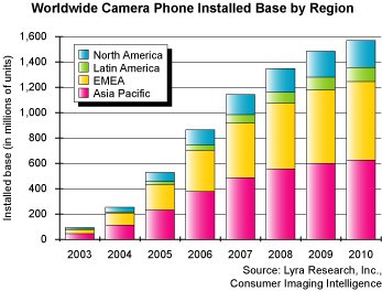
Imaging-Resource: Lyra Research forecasts that the installed base of camera phones in the Asia-Pacific region will grow at a compound annual growth rate (CAGR) of 21.9 percent from 2005 to 2010, topping 600 million camera phones in 2010 (see figure):

Thursday, October 12, 2006
Pixart Research Reports
MasterLink Securities published a couple of interesting research reports on Pixeart business.
The big report is here with a recent status update here.
Some excepts from the report regarding Pixart collaboration with Mediatek and TI:
"PixArt entered camera phone chipset (sensor plus DSP) market in 2004, targeting at VGA level camera phone, and this product accounted for 8% of overall sales in 2004. PixArt’s camera phone chipset was collocated with MediaTek’s baseband to sell to China market in 2Q05, leading to its revenue from camera phone chipset growing 691% to NT$1.28bn in 2005, accounting for 43% of total sales in 2005. Camera phone chipset thus became PixArt’s growth driver in 2005.
However, China government prohibited “White brand” handset in 1H06, leading to PixArt’s shipment for camera phone chipset shrinking to only around 1mn units monthly in 1H06. PixArt is thus aggressively cooperating with UMC to lead in CMOS 4T process to enter MEGA pixel market and we expect this new product to successfully enter mass production in 2H06. Moreover, PixArt has designed in its camera phone chipset into TI’s supply chain. We expect PixArt’s camera phone chipset to start shipping to Taiwan’s handset ODM through collocated with TI’s baseband in 2H06. We thus believe PixArt’s camera phone chipset will regain growth momentum in 2H06 and expect to see 40% sales growth in 2007, despite we estimate the sales from this product line would decrease 27% in 2006 due to poor performance in 1H06."
About optical mouse sensors:
"PixArt launched optical mouse sensor in March 2002 and this product became PixArt’s growth driver in 2003. However, due to the IP lawsuit with Agilent and heavy competition with several new suppliers such as Sunplus, PixArt’s optical mouse sensor sales sequentially dip in 2004 and 2005. Currently, Avago (previous Agilent’s IC division) is the leader among mouse sensor suppliers with around 50% to 60% market share, and PixArt is the second leader with around 20% market share.
We expect to see PixArt’s mouse sensor return growth trend in 2006 and 2007 due to the lawsuit settlement with Agilent on 14th July 2006 and the expected launch for new product, laser mouse sensor. After the lawsuit settlement, PixArt can ship its mouse sensor to America and we expect Logitech, the global mouse leader, will increase the adoption rate for PixArt’s mouse sensor thanks to its peering performance to Avago and lower price. Moreover, laser mouse sensor is expected to be a new growth driver for PixArt’s mouse sensor business in 2007, but we estimate the contribution is little due to price still too high to accept for consumers. We thus estimate PixArt’s mouse sensor sales would sequentially grow 8% in 2006 and 2007."
Also, there are two interesting market forcast graphs:


Other interesting reports on this site:
Largan Presision report on camera optics,
Genius Electronic report on camera lens business,
Premier Image Technology reports 1 , 2 and 3 on camera business,
Sunplus reports 1 , 2 and 3 on ISP, among other things.
The big report is here with a recent status update here.
Some excepts from the report regarding Pixart collaboration with Mediatek and TI:
"PixArt entered camera phone chipset (sensor plus DSP) market in 2004, targeting at VGA level camera phone, and this product accounted for 8% of overall sales in 2004. PixArt’s camera phone chipset was collocated with MediaTek’s baseband to sell to China market in 2Q05, leading to its revenue from camera phone chipset growing 691% to NT$1.28bn in 2005, accounting for 43% of total sales in 2005. Camera phone chipset thus became PixArt’s growth driver in 2005.
However, China government prohibited “White brand” handset in 1H06, leading to PixArt’s shipment for camera phone chipset shrinking to only around 1mn units monthly in 1H06. PixArt is thus aggressively cooperating with UMC to lead in CMOS 4T process to enter MEGA pixel market and we expect this new product to successfully enter mass production in 2H06. Moreover, PixArt has designed in its camera phone chipset into TI’s supply chain. We expect PixArt’s camera phone chipset to start shipping to Taiwan’s handset ODM through collocated with TI’s baseband in 2H06. We thus believe PixArt’s camera phone chipset will regain growth momentum in 2H06 and expect to see 40% sales growth in 2007, despite we estimate the sales from this product line would decrease 27% in 2006 due to poor performance in 1H06."
About optical mouse sensors:
"PixArt launched optical mouse sensor in March 2002 and this product became PixArt’s growth driver in 2003. However, due to the IP lawsuit with Agilent and heavy competition with several new suppliers such as Sunplus, PixArt’s optical mouse sensor sales sequentially dip in 2004 and 2005. Currently, Avago (previous Agilent’s IC division) is the leader among mouse sensor suppliers with around 50% to 60% market share, and PixArt is the second leader with around 20% market share.
We expect to see PixArt’s mouse sensor return growth trend in 2006 and 2007 due to the lawsuit settlement with Agilent on 14th July 2006 and the expected launch for new product, laser mouse sensor. After the lawsuit settlement, PixArt can ship its mouse sensor to America and we expect Logitech, the global mouse leader, will increase the adoption rate for PixArt’s mouse sensor thanks to its peering performance to Avago and lower price. Moreover, laser mouse sensor is expected to be a new growth driver for PixArt’s mouse sensor business in 2007, but we estimate the contribution is little due to price still too high to accept for consumers. We thus estimate PixArt’s mouse sensor sales would sequentially grow 8% in 2006 and 2007."
Also, there are two interesting market forcast graphs:

Other interesting reports on this site:
Largan Presision report on camera optics,
Genius Electronic report on camera lens business,
Premier Image Technology reports 1 , 2 and 3 on camera business,
Sunplus reports 1 , 2 and 3 on ISP, among other things.
Saturday, October 07, 2006
Omnivision Launches 2um Pixel Generation
Sys-Con Media: Omnivision launched its 2um pixel generation CameraChip sensor. Being 1.3MP sensor in 1/5-inch optical format, the OV9660 enables a 25 percent thinner camera module.
Based on OmniVision's proprietary OmniPixel2 technology platform, the new pixel architecture is claimed to significantly increase signal-to-noise ratio and perform exceptionally well in low-light conditions.
The OV9660 comes in CSP and COB packages and is currently available for sampling.
Based on OmniVision's proprietary OmniPixel2 technology platform, the new pixel architecture is claimed to significantly increase signal-to-noise ratio and perform exceptionally well in low-light conditions.
The OV9660 comes in CSP and COB packages and is currently available for sampling.
Tuesday, October 03, 2006
Omnivision Reduces TSMC Orders
Digitimes: The sources cited OmniVision's decreased orders with TSMC. OmniVision's orders for TSMC in August and September decreased significantly compared to July, the sources added.
Subscribe to:
Posts (Atom)