Since someone just pointed out that the Pixim weblink in the ISW vendor list was dead, I decided to put up Pixim datasheets next. These are different from most because Pixim sold a chipset that included the sensor and a matching processor to turn the chip outputs (basically timing data) into digital image data. Pixim also made several demonstration cameras. Sony bought Pixim in 2012 and stopped making Pixim-type chips a couple of years later because they felt they had a better way to do HDR imaging. The debate continues.
Saturday, September 30, 2023
Friday, September 29, 2023
Omnivision announces new sensor for security and surveillance applications
OMNIVISION Announces New Low-power, Enhanced-performance 2MP Image Sensor for Security Surveillance Cameras
The OS02N features a 2.5-micron enhanced-performance FSI pixel with on-sensor DPC for higher sensitivity, performance and reliability while remaining cost-effective
SANTA CLARA, Calif. – September 27, 2023 – OMNIVISION, a leading global developer of semiconductor solutions, including advanced digital imaging, analog, and touch & display technology, today announced the new OS02N, a 2-megapixel (MP) frontside illumination (FSI) image sensor with optimized defective pixel correction (DPC) algorithm for higher sensitivity, improved performance and increased reliability for IP and HD analog security cameras, including professional surveillance and outdoor home security cameras. The OS02N supports always-on with its low-power capability.
“Customers need high-performing security cameras that produce sharp, high-resolution images with low power consumption for extended battery life. The OS02N meets these requirements and is also a cost-effective solution,” said Cheney Zhang, senior marketing manager, OMNIVISION. “The OS02N uses FSI technology, which has a large pixel size for better quantum efficiency and excellent signal-to-noise ratio, resulting in high sensitivity in low-light conditions and dramatically improved image quality and performance. It has a 1/3.27-inch optical format and is designed to be pin-to-pin compatible with our OS04L and OS04D image sensors.”
The OS02N features a 2.5-micron pixel based on OMNIVISION’s OmniPixel®3-HS technology. This enhanced-performance, cost-effective solution uses FSI technology for true-to-life color reproduction in both bright and dark conditions. Optimized DPC algorithm improves sensor quality and reliability above and beyond standard devices by providing real-time correction of defective pixels that can result throughout the sensor’s life cycle, especially in harsh operating conditions. The OS02N features 1920x1080 resolution at 30 frames per second (FPS).
The OS02N supports MIPI and DVP interfaces. It is sampling now and will be in mass production in Q1 2024. For more information, contact your OMNIVISION sales representative: www.ovt.com/contact-sales.
Thursday, September 28, 2023
Sheba Microsystems MEMS-based lens athermalization solution
Sheba Microsystems Launches Revolutionary MEMS Autofocus Actuator for Active Athermalization in Embedded Vision Cameras
Breakthrough µPistons™ technology uniquely solves decades-long embedded vision camera industry’s problem of lens thermal expansion. Novel product unlocks unparalleled resolution and consistent high-quality imaging performance for automotive, action, drone, mobile robotics, security and surveillance, and machine vision cameras.
TORONTO--(BUSINESS WIRE)--Sheba Microsystems Inc., a global leader in MEMS technologies, today announced the launch of its revolutionary new product, the MEMS Autofocus Actuator for Active Athermalization in Embedded Vision Cameras used in automotive, action, drones, machine vision, security and surveillance, and mobile robotics.
The first-of-its-kind solution tackles the long-standing industry problem of embedded vision cameras’ inability to maintain image quality and focus stability during temperature fluctuations as optics undergo thermal expansion.
While smartphones use autofocus actuators and electromagnetic actuators including voice coil motors (VCMs), these actuators are unreliable for achieving active athermalization in embedded vision cameras due to extreme environmental conditions. Embedded vision camera optics are also 30 times larger than smartphone optics. Other autofocus systems in-market such as tunable lenses lack thermal stability and compromise optical quality.
“MEMS actuators are fast, precise, and small in size, and are actually uniquely suited to solve thermal expansion issues, because they are thermally stable and maintain consistent performance regardless of temperature changes,” said CEO and co-founder Dr. Faez Ba-Tis, PhD. “Because of these known advantages, there have been previous industry attempts at incorporating MEMS actuators into cameras, but because they failed drop tests they were quickly abandoned. Sheba’s new design solves for all of these previous blockers, which opens up limitless possibilities for embedded vision camera innovation.”
Sheba’s proprietary technology compensates for thermal expansion by uniquely moving the lightweight sensor, instead of moving the lenses. The silicon-based MEMS actuator platform actuates the image sensor along the optical axis to compensate for thermal expansion in the optics. The weight of the image sensor represents only 2-3 % of the optical lens weight, which makes it easier to handle, enabling ultra-fast and precise autofocus performance even when temperatures fluctuate.
Sheba’s novel piston-tube electrode configuration takes advantage of a larger capacitive area, allowing for substantial stroke and increased force. In contrast to traditional MEMS comb-drive electrode configuration, Sheba’s µPistons™ design makes the MEMS actuators uniquely resilient against severe shocks, since the electrodes are well-supported and interconnected with each other.
Sheba’s new MEMS actuator has successfully passed drop tests as well as other reliability tests, including thermal shock, thermal cycling, vibration, mechanical shock, drop, tumble, and microdrop tests. It is also highly rugged, which helps maintain image focus during high shocks in action cameras or machine vision environments.
“Digital camera technologies are increasingly used in almost every aspect of our lives,” said Ba-Tis. “From sharing photos of our travels in social media, to experiencing new artificial intelligence innovations powered by machine vision, and accelerating the deployment of autonomous vehicles in our communities, high quality images are imperative to not only capture our most memorable events, but to also keep us safe. In situations where split-second decisions are critical, image quality becomes paramount.”
Sheba’s MEMS actuator offers lens design flexibility and is suitable for near and far-field imaging. It is easily integrated into existing systems and scaled up on mass production tools for automotive, action, drone, mobile robotics, security and surveillance, and machine vision cameras.
Sheba is offering evaluation kits to interested customers, so they can test and evaluate the new product in their own labs to ensure the reliability of the technology. The kit includes camera samples, a daughter board with the MEMS driver, interposer, and camera test jig to perform mechanical reliability tests, software, and user manual.
To learn more about Sheba Microsystems or to order an evaluation kit for your organization, visit www.shebamicrosystems.ca.
Wednesday, September 27, 2023
EETimes article on PixArt Imaging's "smart pixel" sensor
Link: https://www.eetimes.com/smart-pixel-optical-sensing-exerting-ai-in-pixels-level/
Smart Pixel Optical Sensing – Exerting AI in Pixels Level
The PAC9001LU Smart Pixel Optical Sensing Chip is a Computer Vision ASIC that fits as an always-on motion sensor by leveraging the novel AI-driven pixel architecture into the sensor array design. Based on a CMOS Image Sensor rolling shutter structural design with an array of 36 x 16 pixels, it can support a high frame rate of up to 1000Hz to facilitate image capturing of fast-moving object applications. The design of AI in pixels integrates a frame comparing circuit with AI-powered algorithms to compute differences in pixel luminosity within a configurable image area. It directly provides analog frame differences and event info in Pixel Differences Mode and supports Smart Motion Detection Mode to eliminate the complex image signal processing in the processor. The partial array sensing, such as configurable ROI region, provides supple custom scene capturing for the needs of AIoT edge applications.

PAC9001LU directly handles the digital conversion of raw image signals. It computes the image subtraction difference between two frames internally in the chip to provide the difference of each pixel in an 8-bit data format. This 8-bit data size is relatively small compared to the raw image data of a whole pixel array, which can effectively reduce data transmission bandwidth and latency issues.

The PAC9001LU chip is in a W2.5 x L2.6 x H0.43 mm3 CSP package body (excluding solder balls). A recommended matching lens set, LST0-2621 is also available to form a complete module when assembled with the PAC9001LU chip and comes in a size of W3.79 x L3.63 x H1.67 mm3 (height is including guide pin).

- The low-power consumption during the Smart Motion Detection Mode that comes with intelligent informative is the most remarkable building block worthwhile in enabling AI applications. As compare to PIR or CMOS Image Sensor (CIS), higher power consumption is required for further data processing in system level.
- The high report rate, which can go up to 1000Hz can achieve motion detection with fast-moving objects, which outperforms the PIR or conventional CIS.
- The PAC9001LU is more robust with reliable performance. It has fewer false alarms detecting motion and higher immunity to temperature interference. The external environment factors, such as bright and hot sunlight from outdoors, the indoors thermal noise from heated devices are not affecting its sensing performance. The built-in algorithms can eliminate interferences like background noise too.
- The small form factor of the complete PAC9001LU sensor module, including the lens set, can nicely fit into the slim bezel ID design.
- The traditional PIR sensors are usually required not to be shielded by plastics or glass front-facing cover, which may impact the detection of thermal IR radiation. Whereas the PAC9001LU solution does not have the restraint of having a front cover of any materials and still can keep the motion sensing quality, even placing the motion sensing device indoors looking out from the glass window is possible. With the cover protection, the PAC9001LU is less prone to external damage.


PAC9001LU sensor can support low-light sensing in low or no-light conditions, which is very suitable for use in a dark environment, such as a basement.

The PAC9001LU can cater to the need for in-chip high-speed motion detection, eliminating the external controller processing.
In addition to motion sensing, the PAC9001LU sensor can provide the coordinate information of a targeted moving object that is in sync with each pixel differences image data.

Sunday, September 24, 2023
Job Postings - Week of 24 Sep 2023
To start the revised posting scheme,here are recently posted jobs from Apple and onsemi:
Apple
|
Image Sensor Validation Engineer |
Cupertino, California, USA |
|
|
Sensor Process Engineer - Camera Hardware |
Cupertino, California, USA |
|
|
Image Sensor Validation Engineer |
Grenoble, Isere, France |
|
|
Sensor Process Engineer |
Kanagawa, Kanagawa-ken, Japan |
|
|
Sensor Process Engineer |
Cupertino, California, USA |
|
|
Pixel Development Engineer |
Pasadena, California, USA |
|
|
Technical Program Manager (TPM), Image Sensor |
Tokyo, Tokyo-to, Japan |
onsemi
|
Strategic Platform Architect – Image Sensors |
San Jose, California, USA |
|
|
Technical Project Manager – Image and Depth Sensors |
Haifa, Israel |
|
|
Sr Director Bracknell Design Center |
Bracknell, Berkshire, UK |
|
|
Summer 2024 Analog/Digital Verification Intern |
San Jose, California, USA |
|
|
Process Design Kit Development Staff Engineer |
Scottsdale, Arizona, USA |
Let us know if you would like us to check out a specific company or if you know of jobs we should post.
Job Posting Update
In order to eliminate the delays involved in reproducing jobs listings in detail, the method of reporting is changing. Starting today, this Jobs Update will be a report on job listings rather than the listings themselves. Even in the apparent slowdown in the job market, the number of listings is still quite large and the backlog of listings that might be of interest is much larger.
To manage this situation, we will proceeds as follows: for the next few weeks, the posting will focus each week on a small number of employers with multiple openings. Relevant job titles with their locations and original listing links will be posted. The job descriptions will no be included simply because they are all so long - click the links to see the details. Please note that we will attempt always to link to the original listing on the employer website, not to job boards.
Weekly job lists in ISW will continue to have individual links for four weeks but since many jobs remain unfilled longer than that, the older postings will be held in an archive for a year. The link to the archive is positioned below the four week links.
Initially, some of the postings may be several months old but, at some point, our listings will catch up with the backlog and each weekly posting will include only recent additions.
Conference List - October 2023
Optica Laser Congress and Exhibition - 8-10 Oct 2023 - Tacoma, Washington, USA - Website
IEEE International Conference on Image Processing - 8-11 Oct 2023 - Kuala Lumpur, Malaysia - Website
244th Electrochemical Society Meeting - 8-12 Oct 2023 - Gothenburg, Sweden - Website
SPIE/COS Photonics Asia - 14-16 Oct 2023 - Beijing, China - Website
ASNT Annual Conference - 22-26 Oct 2023 - Houston, Texas, USA - Website
SPIE Photonex - 24-26 Oct 2023 - Glasgow, Scotland, UK - Website
BioPhotonics Conference - 24-26 Oct 2023 - Online - Website
OPTO Taiwan - 25-27 Oct 2023 - Taipei, Taiwan - Website
Return to Conference List index
Saturday, September 23, 2023
Conference List Announcement
Image Sensors World is pleased to introduce its compiled list of conferences and exhibitions that include image sensor topics and products. The range includes everything from device physics and designs to applications and test. Included are on-site meetings, on-line webinars and various sorts of hybrid and archived events.
Because many meetings keep the presented materials available on-line for extended periods, each event will remain in the listings for one year or until the next session of the event occurs, whichever is shorter. New events will be listed as soon as they are announced and grouped by the month the event is scheduled to begin.
The ISW list will be broader than the individual posts announcing events that ar4e focused on image sensor such as the IISW or some of the IEEE meetings. Those posts will continue to assure that ISW readers are aware of them in time to submit papers or make travel plans.
Building the list will take some time so the postings will be added in chronological order with those scheduled soonest first. Listings will be brief, giving the sponsor, event name, location, dates and a link to the event website. Note that often the links change as the date of the event approaches. Occasionally, additional information will be supplied that affects who can attend - security clearance or membership requirements, for example.
Most events require payment for attendance to technical sessions and some charge for exhibits. These listings will not include the costs because those are often contingent on time, membership, discounts and other factors. See the event websites for registration details.
Finally, if you are reading the listings looking for opportunities to exhibit your products, those with associated exhibitions will usually have exhibitor information sections on their websites. Please consult them as early as possible. Many popular shows are sold out long before the event begins and some require reservations years in advance.
Feel free to post comments on the shows - your experiences or plans - and let us know if you are aware of an event ISW should list.
The index to the monthly lists is here.
Friday, September 22, 2023
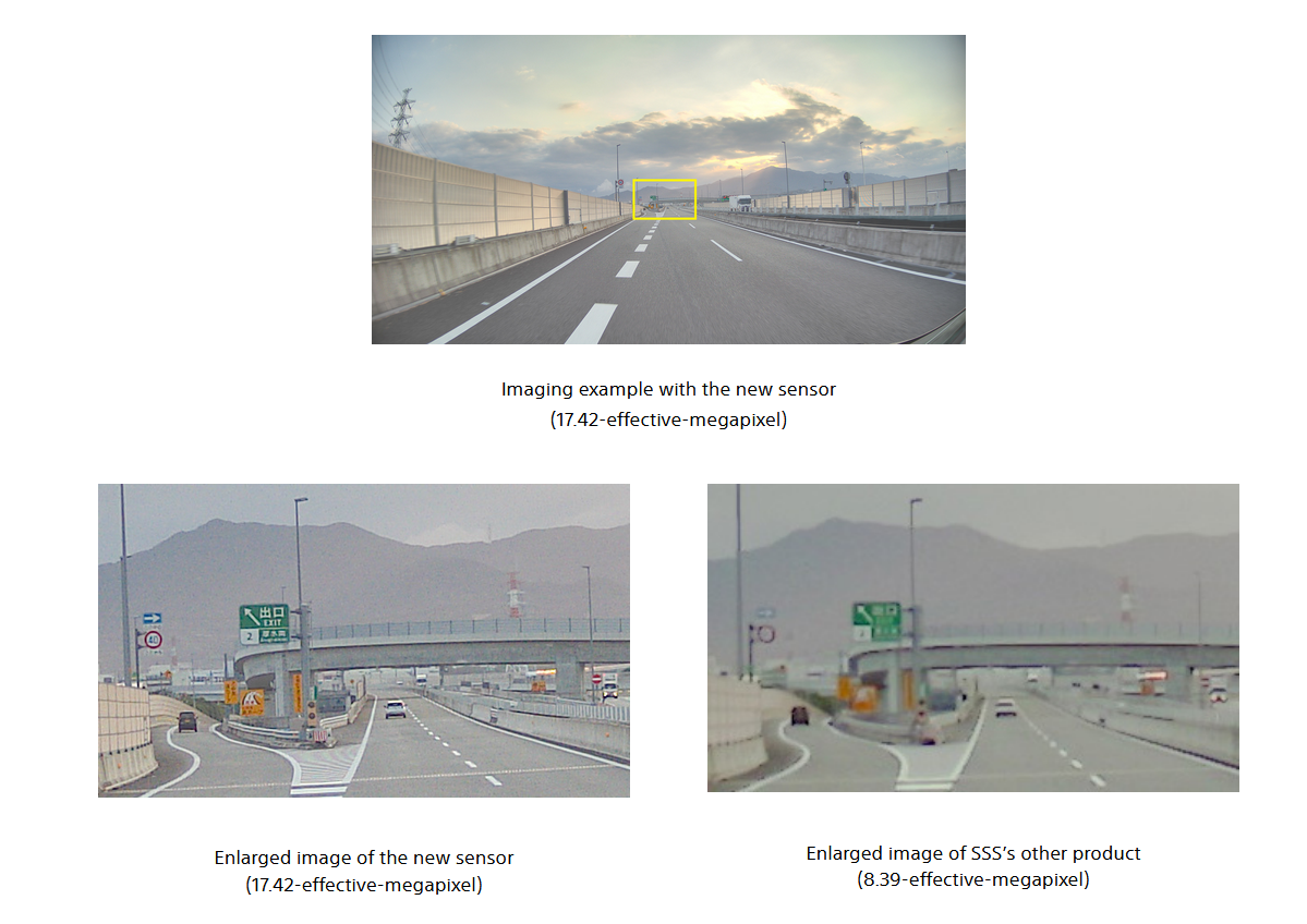
Sony announces IMX735 17.42MP Automotive CIS
Press release: https://www.sony-semicon.com/en/news/2023/2023091201.html
Sony Semiconductor Solutions to Release CMOS Image Sensor for Automotive Cameras with Industry-Leading 17.42-Effective Megapixels
Delivering sophisticated sensing and recognition performance and contributing to safe, secure automated driving
Atsugi, Japan — Sony Semiconductor Solutions Corporation (SSS) today announced the upcoming release of the IMX735, a new CMOS image sensor for automotive cameras with the industry’s highest pixel count, at 17.42 effective megapixels. The new sensor product will support the development of automotive camera systems capable of sophisticated sensing and recognition performance, thereby contributing to safe, secure automated driving.
For automated systems to deliver automated driving, they must offer sophisticated, high-precision sensing and recognition performance, encompassing all 360 degrees of the environment around the vehicle. Accordingly, there is considerable demand for image sensors that can help achieve this level of performance and support the development of more advanced automotive camera systems.
The new sensor product achieves the industry’s highest pixel count of 17.42 effective megapixels, enabling high definition capture of far-off objects. Moreover, automated driving systems often use automotive cameras in combination with LiDAR and other sensing systems. While typical CMOS image sensors readout signals output from pixels one vertical line at a time, this product outputs signals horizontally, one row at a time. This means that automotive cameras employing this sensor can more easily synchronize with mechanical scanning LiDAR, since their laser beams also scan horizontally. This better synchronization will improve the sensing and recognition capabilities of the automated driving system as a whole.
Furthermore, the new sensors’ improved saturation illuminance, made possible by a proprietary pixel structure, and unique exposure method yield a wide dynamic range of 106 dB even when simultaneously employing high dynamic range (HDR) imaging and LED flicker mitigation. The dynamic range is even higher, at 130 dB, when using dynamic range priority mode. This creative design helps suppress highlight blowouts even in backlit conditions, enabling more precise object capture in road environments with significant differences in brightness, such as tunnel entrances and exits.
Main Features
■Long-distance recognition delivered by industry-leading 17.42 megapixels
Thanks to the industry’s highest pixel count of 17.42 effective megapixels, the new sensor is capable of high definition capture, extending the object recognition range to greater distances and thereby allowing better detection of road conditions, vehicles, pedestrians and other objects. Early detection of far-away objects while driving helps make automated driving systems safer.
■Horizontal pixel signal output for easier synchronization with mechanical-scanning LiDAR
When reading signals from pixels, CMOS image sensors generally do so in a vertical direction one line at a time. This product, on the other hand, employs a readout method that outputs signals horizontally one row at a time, making it easier to synchronize with mechanical-scanning LiDAR, which also uses a horizontal scanning method. This means that the information output from automotive cameras equipped with this product can be integrated with LiDAR information downstream on the system. This will improve the sensing and recognition capabilities of the automated driving system as a whole.
■Wide dynamic range even during simultaneous use of HDR and LED flicker mitigation
In automobile driving, objects must be precisely detected and recognized even in road environments with significant differences in brightness, such as tunnel entrances and exits. Automotive cameras are also required to suppress LED flicker, even while in HDR mode, to deal with the increasing prevalence of LED signals and other traffic devices. The proprietary pixel structure and unique exposure method of this product improves saturation illuminance, yielding a wide dynamic range of 106 dB even when simultaneously employing HDR and LED flicker mitigation (when using dynamic range priority mode, the range is even wider, at 130 dB). This design also helps reduce motion artifacts generated when capturing moving subjects.
■Compliant with standards required for automotive applications
The product is qualified for AEC-Q100 Grade 2 automotive electronic component reliability tests by mass production. Also, SSS has introduced a development process compliant with the ISO 26262 road vehicle functional safety standard, at automotive safety integrity level ASIL-B(D). This contributes to improve automotive camera system reliability.
■Cybersecurity required for automotive applications (optional)
The product can support cybersecurity features such as camera authentication via a public-key algorithm to confirm CMOS image sensor authenticity, image authentication to detect any tampering with acquired images, and communication authentication to detect any tampering with control communications.

Thursday, September 21, 2023
Texas Instruments Documentation
Texas Instruments made (mostly) area CCDs using the virtual-phase architecture invented by Jerry Hynecek in their Central Research Lab. Some later devices, designated "Impactron" incorporated a high-voltage shift register that provided electron multiplication. TI made these devices until 2011 when their fab in Aizu-wakamatsu, Japan, was heavily damaged in an earthquake. The CCD line was never restarted.
You may notice that the archive includes a data sheet for the TIVICON silicon vidicon camera tube. Truly, TI made an imaging vacuum tube before it made solid-state sensors. It was built for an Air Force forward-looking infrared (FLIR) system that flew over the jungles of Vietnam making thermal images of people among the trees. The silicon vidicon looked at a spinning line of infrared LEDs (another TI product) to produce a windshield-wiper-shaped image that was displayed on a video monitor. I ran the lab that tested these tubes and I wrote the data sheet included in the archive to start TI on commercial sales of the tubes. I was gone before TI introduced CCDs but my boss, Frank Skaggs, moved to that program.
Link to the TI folder
Return to the Documentation List
Image Sensor Documentation Archive
We are pleased to introduce a new feature of the ISW blog, an archive of data sheets and other documents related to image sensor products. A recent survey of blog readers indicated that many of you would like access to a location where both historical and current data sheets, application notes, test data and other documents describing image sensors released to the market are available for download. The new archive will provide this.
Image sensors have been made by over 200 companies since manufacturing began in the early 1970s and new ones appear almost every day now. I will attempt to both fill in the past and keep the archive current but catching up will take a while. Please comment if you have priorities you would like me to consider. Also comment if you have recollections that might interest the newer members of the image sensor community.
All of the documents will be stored on a Google Drive account with open access. This means that documents that are export-controlled, mostly for thermal sensors, will not be included. To get to the Drive folders, you need only to click a company link on the blog post that comes up when you select "Image Sensor Documentation" from the list on the left of the blog front page. Download whatever you like.
If you have anything you would like to contribute, send me an e-mail and we can make an arrangement. While we are interested in more than just data sheets, we can't post any company confidential information even if the company is out of the image sensor business or no longer exists.
As I add new companies to the archive, I will post announcements with a link to the company folder and a little background on the company. Again, feel free to comment if you have something interesting to add. Note that the companies and their documents will be identified by the company name in use when each sensor was introduced. Thus, companies like OnSemi may have products under other names going all the way back to Photobit or IMEC or Kodak.
The first company up is Texas Instruments, active 1978-2011, making virtual-phase and electron-multiplying sensors invented by Jerry Hynecek. The post with the link to the TI documents is here.
Image Sensor Documentation List
The ISW Blog documentation folders contain documents for image sensors from these companies:
Excelitas Announcement Document Archive
Foveon Announcement Document Archive
PerkinElmer Announcement Document Archive
Pixim Announcement Document Archive
Reticon Announcement Document Archive
SITe Announcement Document Archive
Tektronix Announcement Document Archive
Texas Instruments Announcement Document Archive
Wednesday, September 20, 2023
Photonis is now ExoSens
PHOTONIS GROUP BECOMES EXOSENS
PRESS RELEASE
MÉRIGNAC – SEPTEMBER 20th 2023
PHOTONIS GROUP a global leader of highly differentiated technology for detection, imaging and light, held by Groupe HLD since 2021 is deeply transforming by developing adjacent technologies, expanding to particles detection markets. Following that strategy, the group has acquired four companies (Xenics, Proxivision, Telops and Elmul) since December 2022. Worldwide leader for image intensifier tubes, the company has diversified its technologies and products portfolios with the ambition to become the worldwide leader in detection and imaging technologies. To illustrate that strategy, PHOTONIS GROUP becomes EXOSENS.
Proposing electro-optic devices covering the full optical spectrum from UV to LWIR in addition to electron, ion, neutron and gamma detectors, EXOSENSaddresses four markets which are lifescience, industrial control, nuclear energy and defense. The company takes benefits of positive dynamics in each of these four verticals, such as enhanced diagnosis demand, factory automation, small modular reactors deployment and defense budget increase.
Jean-Hubert Vial, partner at Groupe HLD said: “It’s an important step for Photonis Group. By becoming EXOSENS, the company clearly anchors its position as high-end technology provider to serve high growing commercial and defense markets for more sustainability and safety”
Jérôme Cerisier, CEO of the new group said: “EXOSENS means “to detect, to see and to give meaning to what is beyond”. It perfectly reflects what we are doing, we reveal the invisible, we sense the world to make it safer. With EXOSENS, we aim to share our common values throughout the whole organization, to integrate new companies and colleagues and to always offer high performances products to meet customers satisfaction.”
Operationally, legal entities will keep their existing names. The four product brands Photonis (for intensified products, nuclear and mass spectrometry detectors), Xenics (for infrared sensors and cameras), Elmul (for electron detectors) and Telops (for hyperspectral and cooled infrared camera) will continue to be deployed and promoted in their markets.
ABOUT EXOSENS:
Accompanied by Groupe HLD since 2021, EXOSENS is a high-tech company, with more than 85 years of experience in the innovation, development, manufacture and sale of technologies in the field of particles and photo detection and imaging. Today, it offers its customers detectors and detection solutions: its travelling wave tubes, advanced cameras, neutron & gamma detectors, instrument detectors and light intensifier tubes allow EXOSENS to respond to complex issues in environments extremely demanding by offering tailor-made solutions to its customers. Thanks to its sustained and permanent investment, EXOSENS is internationally recognized as a major innovator in optoelectronics, with production and R&D carried out on 9 sites, in Europe and North America and over 1 500 employees.
International Image Sensors Workshop 2023 Papers are Available Online
Papers from the recent International Image Sensor Workshop (IISW) 2023 held in Crieff Scotland are now available on the International Image Sensor Society website:
Link: https://imagesensors.org/2023-papers/
An exciting lineup of invited talks, posters, and papers over nine different sessions; go check it out!
Session 1 3D Stacking and Small Pixels
Session 2 Noise
Session 3 Pixel Design & Process Technology
Session 4 HDR and Automotive
Session 5 Smart and Event-based Imagers
Session 6 Beyond Visible & Scientific Imaging
Session 7 Speciality and New Applications
Session 8 SPAD Devices
Session 9 Time of Flight
OmniVision's new automotive image sensor OX08D10
OMNIVISION Announces New TheiaCel™ Technology and Automotive Image Sensor for LED-Flicker-Free Exterior Cameras
Announced at AutoSens Brussels, the OX08D10 is a small, low-power-consumption image sensor that features OMNIVISION’s new TheiaCel™ technology for superior image quality regardless of lighting condition
BRUSSELS, Belgium – September 19, 2023 – OMNIVISION, a leading global developer of semiconductor solutions, including advanced digital imaging, analog and touch & display technology, today debuted its OX08D10 8-megapixel (MP) CMOS image sensor with TheiaCel™ technology at AutoSens Brussels. The new solution enhances automotive safety by providing enhanced resolution and image quality in exterior cameras for advanced driver assistance systems (ADAS) and autonomous driving (AD).
The OX08D10 features industry-leading lowlight performance and low power consumption in a compact size that is 50% smaller than other exterior cabin sensors in its class. It is the first image sensor that features OMNIVISION’s new 2.1-micron (µm) TheiaCel™ technology, which harnesses the capabilities of next-generation lateral overflow integration capacitors (LOFIC) and OMNIVISION’s DCG™ high dynamic range (HDR) technology to eliminate LED flicker regardless of lighting conditions. TheiaCel™ enables the OX08D10 to achieve HDR image capture at up to 200 meters. This range is the sweet spot for delivering the best balance between SNR1 and dynamic range and is optimal for automotive exterior camera applications.
“The new OX08D10 image sensor provides automotive OEMs with one device that combines all of the most important features, including low-light performance, LED flicker mitigation (LFM), small size and low power, eliminating the need for our customers to make performance/design compromises to address LED flicker, as they have in the past,” said Paul Wu, automotive product marketing manager, OMNIVISION. “Additionally, we are excited to debut our new TheiaCel™ technology at AutoSens this year. TheiaCel™ brings a new era to single-exposure HDR in an easy-to-implement solution that yields dramatic improvements in image quality.”
“LFM, HDR and high resolution have become essential prerequisites in modern automotive image sensors to achieve higher autonomy vehicles,” said Anas Chalak, technology & market analyst, Imaging at Yole Intelligence, part of Yole Group. “OMNIVISION’s TheiaCel™ DCG + LOFIC solution fulfill these criteria, aligning with the trend of implementing more exterior cameras per car in the upcoming years. By 2028, we expect the ADAS camera market volume to reach around 105M units and the overall automotive image sensor market to expand to $3.7 billion, experiencing a CAGR22-28 of 8.7%1.”
In the automotive market, flicker from LED traffic lights poses a serious challenge for imaging solutions, preventing ADAS and AD systems from correctly detecting lighted traffic signs. The industry has been clamoring for a solution that could be easily integrated into a CMOS image sensor to meet this challenge. Some previous approaches, while achieving satisfactory LFM, have resulted in reduced image quality, especially at high automotive temperatures.
OMNIVISION’s new 2.1µm single-pixel TheiaCel™ technology delivers high LFM without sacrificing image quality. TheiaCel™ leverages next-generation LOFIC capabilities together with the proven strength of OMNIVISION’s proprietary HDR technology (patented DCG and split-diode technology), which captures extremely high-contrast scenes for optimum content and image quality. OMNIVISION’s TheiaCel™ DCG + LOFIC solution achieves a wider dynamic range than earlier single-exposure HDR architectures.
The new OX08D10 achieves overall superior performance in key areas compared to its non-LOFIC-based predecessor – in particular, its LFM dynamic range is 3.3x higher and total dynamic range nearly 3x higher. It features upgraded cybersecurity to comply with the newest MIPI CSE version 2.0 standards, which adds functional safety to automotive image sensor data streams. The TheiaCel™ device features OMNIVISION’s a-CSP™ package technology for the smallest possible solution. Samples are available now, and the OX08D10 will be in mass production in the second half of 2024. For more information, contact an OMNIVISION sales representative: www.ovt.com/contact-sales.
About OMNIVISION
OMNIVISION is a global fabless semiconductor organization that develops advanced digital imaging, analog and touch & display solutions for multiple applications and industries, including mobile phones; security and surveillance; automotive; computing; medical; and emerging applications. Its award-winning innovative technologies enable a smoother human/machine interface in many of today’s commercial devices. Find out more at www.ovt.com.
1 Imaging for Automotive report, Yole Intelligence, 2023.
OMNIVISION®, TheiaCel™, DCG™, a-CSP™ and the OMNIVISION logo are trademarks or registered trademarks of OMNIVISION. All other trademarks are the property of their respective owners.
Monday, September 18, 2023
Imaging Sensors and Systems @ EI 2024 - Abstract Deadline September 30
Imaging Sensors and Systems at EI 2024: Jan 21-25
IS&T is currently accepting submissions for its 2024 Electronic Imaging Symposium. Comprised of 18 conferences spanning one to four days, of most interest to the sensor community may be Imaging Sensors and Systems 2024, which focuses on a wide range of image sensing topics and brings together researchers, scientists, and engineers working in these fields, offering the opportunity for quick, open access publication of their work.
What makes ISS different?
· Offers a place of exchange and opportunity for quick publication of new work in the areas of solid state detectors, solid state cameras, new optical concepts, image processing, and novel applications.
· Features work from both industry and academia, and includes state-of-the-art presentations by invited keynote speakers complimented by topics covered in several of the short courses, as well as the plenary, demonstration, and poster sessions.
· Includes a mixture of both tutorial and highly advanced research presentations, so that researchers, students, and engineers all can find content that is appropriate to their level of expertise. Some of the conference sessions include overview talks, as well as panel discussions that allow for in-depth Q&A interactions with experts in industry and academia.
· Access to all the EI conferences. Of particular interest may be:
· Autonomous Vehicles and Machines
· Computational Imaging
· High Performance Computing for Imaging
· Image Quality and System Performance
· Image Processing: Algorithms and Systems
· Machine Learning for Scientific Imaging
· Intelligent Robotics and Industrial Applications using Computer Vision
The conference takes place in the Silicon Valley, close to San Francisco Airport, offering proximity to local tech companies and easy transportation options.
Submission options include proceedings paper and presentation only.
Extended submission deadline: 30 September 2023
For other conferences, visit their individual webpage: see all conferences listing
Plenary speaker and other program details will be announced in the next few weeks.
Subscribe to:
Posts (Atom)