
Sunday, September 30, 2018
Omnivision Applies for Patent on Cross-type PDAF with Dual-PD
Omnivision patent application US20180249105 "Image Sensor with Two-Dimensional Split Dual Photodiode Pairs" by Gang Chen, Qin Wang, Duli Mao, and Lindsay Grant proposes cross-type PDAF pixels that are also used for a regular image sensing:

IHS Markit Estimates iPhone Xs Max Cameras Cost at $51.10
IHS Markit estimates Apple iPhone Xs Max camera components cost at $51.10 out of the total BOM of $390:


Saturday, September 29, 2018
Sony Officially Announces Polarization Imagers
Sony officially unveils IMX250MZR / MYR polarization sensitive image sensors. The IMX250MZR monochromatic version is available now, while color IMX250MYR is expected to be available in December 2018. The 5.07MP sensors use 3.45µm global shutter pixel with four-directional polarizer formed on the photodiode:


"With conventional types of polarization sensors, the polarizer is attached on top of the on-chip lens layer (Fig.2), however with Sony Semiconductor Solutions’ polarization sensor the polarizer is formed on chip under the on-chip lens layer (Fig.3). A shorter distance between the polarizer and the photodiode improves the extinction ratio and the incident angle dependence.
Since the polarizer is formed during the semiconductor process, form and formulation of polarizer, uniformity, mass productivity and durability are excellent compared to conventional polarization sensors. Furthermore, Sony Semiconductor Solutions’ Polarization sensor is covered with an anti-reflection layer which helps to reduce reflectance and avoids poor flare and ghost characteristics.
By creating a unique air gap structure in the polarizer, it enables excellent polarization properties and sensitivity in a broad band from visible to near infrared. It also has an advantage of excellent image quality in various light source environments by introducing the world's first anti-reflection layer to reduce flare and ghost for polarization sensor."


The company shows a number of examples where polarization imaging has advantages:


Friday, September 28, 2018
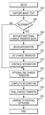
Apple Applies for Patent on Image Sensor Having FWC Beyond Photodiode Capacity
Apple keeps filing continuation applications for its stacked pixel patent filed more than 4 years ago. The most recent continuation is named "Image Sensor Having Full Well Capacity Beyond Photodiode Capacity" by Xiaofeng Fan. The company proposes a selectable single or dual exposure control in a wafer stacked structure with per-pixel interconnects:
"The full well capacity of photodiodes in image sensors generally determines the exposure time, and may also affect the signal to noise ratio and/or the dynamic range of the image sensor. In some embodiments, the full well capacity of the photodiodes in the image sensor may be dynamically adjusted to allow longer exposure times, reducing blooming artifacts in captured images, and to increase the dynamic range of the image sensor. In one embodiment, the image sensor may transfer charge from the photodiode to a storage node one or more times during integration (e.g., the exposure time frame). Transferring the charge during integration may allow the full well capacity of the photodiode to be increased beyond the hardware imposed well capacity. Additionally, because the full well capacity may be varied without changing the hardware of the image sensor, the full well capacity can be dynamically varied allowing the image sensor to adjust to different lighting conditions, image capturing settings (e.g., video or still photographs), as well as allow a user to adjust the exposure time as desired without increasing blooming artifacts.
The storage node 702 may have an increased capacitance to accommodate multiple charge transfers from the photodiode 154. For example, the storage node 702 may be sufficiently large to accommodate double (or more) the capacity of the photodiode 154. This allows the storage node 702 to store charge from multiple charge transfers from the photodiode 154 as the integration time of the photodiode 154 is increased over the hardware implemented full well capacity."


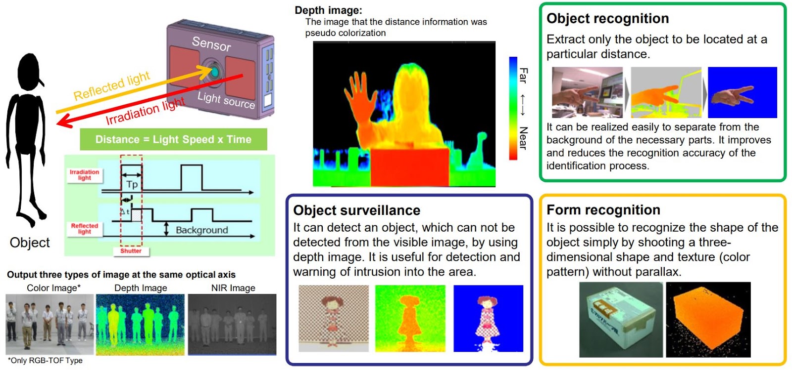
Panasonic, Fujitsu ToF Sensors
Panasonic is developing a 3D ToF image sensor for AI-based advanced driver monitoring systems. The ToF image sensor has 5.6um pixel optimized for high sensitivity at 940nm wavelength to operate under bright sunlight. This sensor is AEC-Q100 Grade2 compliant and is designed to be used for next-generation in-cabin applications such as gesture-based user interfaces and driver monitoring.
The company's ToF web page also shows smartphone and industrial applications for its sensor:


Fujitsu UK offers ToF Camera Development Kit:


The company's ToF web page also shows smartphone and industrial applications for its sensor:


Fujitsu UK offers ToF Camera Development Kit:


Thursday, September 27, 2018
Pioneer Rolls Out LiDAR Lineup, Presents Roadmap
Pioneer announces that from late September, the company will sequentially start shipping three types and four models of 3D-LiDAR sensors, which adopt the MEMS mirror method and differ in measurement distance: “Telescopic LiDAR”, “Medium-range LiDAR” and “Short-range LiDAR.” Pioneer is developing a high-performance, downsizing, lower price 3D-LiDAR using a MEMS mirror, aiming for mass production in the 2020s. Pioneer provided its first sample for testing September 2017 to companies in Japan and overseas.
In response to diverse customer needs, Pioneer is also developing the wobbling scanning method of “Wide-view LiDAR” in addition to the raster scanning method.


In response to diverse customer needs, Pioneer is also developing the wobbling scanning method of “Wide-view LiDAR” in addition to the raster scanning method.


RED 16x8K 60fps Super 35mm Sensors VR Camera
RED introduces a camera for shooting immersive 360 degree VR content featuring 16 fish eye cameras with 8K 60fps Super 35mm Helium sensor each (active area 29.9 x 15.77mm2, 3.65um pixels).


Thanks to AL for the pointer!


Thanks to AL for the pointer!
Wednesday, September 26, 2018
Oculus Quest Features 4 Wide-Angle Cameras
Facebook Oculus announces its next generation stand-alone VR headset - Oculus Quest. While most of its spec is hidden yet, the headset is said to be equipped by 4 wide-angle cameras to enable 6DoF:


ID Quantique Announces Quantum RNG Chip
Geneva, Switzerland-based ID Quantique launches the fruit of its cooperation with SK Telecom - an image sensor-based Quantum Random Number Generator (QRNG) chip - Quantis.
"At its core, the QRNG chip contains a light-emitting diode (LED) and an image sensor. Due to quantum noise, the LED emits a random number of photons, which are captured and counted by the image sensor’s pixels, giving a series of raw random numbers. These numbers are fed to a randomness-extraction algorithm which distills the entropy of quantum origin and makes it available to the user.
Based on a technology concept and patent from IDQ, and designed and manufactured by SK Telekom, the Quantum RNG Chip harnesses true quantum randomness from the shot noise of a light source captured by a CMOS image sensor"


Isorg Raises €24M to Ramp Up Large-Scale Production
ALA News: Isorg, a maker of printed organic photodetectors and large-area image sensors, raises €24M in a Series B round. New Science Ventures (NSV), a US-based investment firm and Bpifrance, through its fund Large Venture, are leading the round alongside Financière Fonds Privés (FFP) and current investors, Sofimac Innovation, CEA Investissement and Dynalim. The Series A round of €7.9M took place in 2014. Isorg’s technology can be used in smartphones, wearables, tablets and laptops, biometrics for homeland security and medical imaging.
The €24M funding will be used to support the qualification steps of its production site based in Limoges, France and continue the development of subsystems ready to be integrated in the various applications. It will support the work to enable large-scale commercialization in the coming years.
“We are heading towards launching the large-scale commercialization of our image sensors and other printed electronics solutions, which are in high demand among manufacturers of consumer electronics and biometric devices,” said Jean-Yves Gomez, CEO and co-founder of Isorg.
Tuesday, September 25, 2018
TechInsights: iPhone XS Max Cameras Cost More than Last Year's Model
TechInsights iPhone XS Max teardown has been updated with the cost analysis of the new model vs the last year iPhone X:
| Components cost estimation | ||
| Apple iPhone XS Max A1921 | Apple iPhone X A1091 | |
| Applications Processor/Modems | $72.00 | $66.22 |
| Battery | $9.00 | $6.46 |
| Connectivity & Sensors | $18.00 | $17.11 |
| Cameras | $44.00 | $42.80 |
| Display | $80.50 | $77.27 |
| Memory | $64.50 | $45.35 |
| Mixed Signal/RF | $23.00 | $23.31 |
| Power Management/Audio | $14.50 | $14.16 |
| Other Electronics | $35.00 | $32.51 |
| Mechanicals/Housings | $58.00 | $45.71 |
| Test/Assembly/Supporting Materials | $24.50 | $24.55 |
| Total | $443.00 | $395.44 |
TechInsights: Apple Increases Number of PDAF Pixels in New iPhones
TechInsights teardown of iPhone Xs reveals that:
"Our early camera teardown effort has been focused on the 12 MP resolution wide-angle camera, promoted as a new, larger sensor with bigger, deeper pixels. The iPhone XS Max wide-angle camera chip is a stacked imager sourced from Sony and features a 7.01 mm x 5.79 mm (40.6 mm2) die size. This compares to 5.21 mm x 6.29 mm (32.8 mm2) for the iPhone 8/X wide-angle camera chips.
We confirmed the iPhone XS Max’s wide-angle camera pixel pitch of 1.4 µm (up from 1.22 µm) and immediately noticed the increased density of Focus Pixels compared to last year’s iPhone 8/X. The term Focus Pixels is Apple’s branding of masked phase detection autofocus (PDAF) pixels and the higher Focus Pixel count translates to more regions available as autofocus points. Focus Pixels were introduced in 2014 for iPhone 6 and at that time featured left and right-masked Focus Pixel pairs. In 2017 Apple moved from a paired to shared Focus Pixel strategy, where top/bottom masked pixels were added and all were evenly distributed within selected rows/columns. Apple has implemented all of its wide-angle Focus Pixels in the green channel."
 |
| 12 MP wide-angle camera image sensor die with removed CFA |
Fujitsu Presents 1,000:1 Image Compression for Driverless Cars
Nikkei: Fujitsu unveils an image compression technology that reduce the file size to 0.1% of the original one, aimed to self-driving applications.
The new algorithm is said to compress data with 1,000:1 ratio, while still maintaining its usability for AI ML algorithms. By reducing the volume of data, cars can send high-resolution images over the internet to data centers in real time.
The new algorithm is said to compress data with 1,000:1 ratio, while still maintaining its usability for AI ML algorithms. By reducing the volume of data, cars can send high-resolution images over the internet to data centers in real time.
Monday, September 24, 2018
Omnivision Unveils 2 Global Shutter Sensors with 3um Pixels
PRNewswire: OmniVision announces two new additions to its family of global shutter sensors—the OG02B1B/OG02B10 and the OV9285. These new sensors are aimed to be cost-effective solutions for consumer and industrial machine vision applications.
“Machine vision applications are experiencing strong growth, fueled by increased demand for industrial automation and new use cases such as augmented reality and virtual reality. Meanwhile, computer vision algorithms are becoming more and more sophisticated, which in turn drives up the performance requirements of image sensors,” said Sanjay Kumar, senior marketing manager at OmniVision. “We are excited to offer these high-resolution and high-performance global shutter image sensors to the machine vision community, enabling new applications and new use cases.”
The 2-megapixel OG02B1B (monochrome) and the OG02B10 (color) image sensors provide 1600 x 1300 resolution in a 1/2.9-inch optical format and a 15-degree CRA to support wide field-of-view lens designs. This combination of color imaging and CRA is excellent for applications such as agricultural drones that must capture high-resolution color images for crop and field monitoring.
The OV9285 provides an even more cost-effective option, with a 1.48-megapixel or 1328 x 1120 resolution, the ability to capture video at 90 fps and an optical format of 1/3.4-inch with a CRA of 9 degrees.
Both sensors are built on 3um OmniPixel3-GS pixel technology. It provides high QE and NIR sensitivity at 850nm and 940nm, which reduces power consumption and extends device battery life.
The OG02B1B, OG02B10 and OV9285 image sensors are available now.

Film-Based Light Sensing Review
University of Toronto repo publishes a Nature paper from January 2017 "Solution-processed semiconductors for next-generation photodetectors" by F. Pelayo García de Arquer, Ardalan Armin, Paul Meredith, and Edward H. Sargent.
"Efficient light detection is central to modern science and technology. Current photodetectors mainly use photodiodes based on crystalline inorganic elemental semiconductors, such as silicon, or compounds such as III–V semiconductors. Photodetectors made of solution-processed semiconductors — which include organic materials, metal-halide perovskites and quantum dots — have recently emerged as candidates for next-generation light sensing. They combine ease of processing, tailorable optoelectronic properties, facile integration with complementary metal–oxide–semiconductors, compatibility with flexible substrates and good performance. Here, we review the recent advances and the open challenges in the field of solution-processed photodetectors, examining the topic from both the materials and the device perspective and highlighting the potential of the synergistic combination of materials and device engineering. We explore hybrid phototransistors and their potential to overcome trade-offs in noise, gain and speed, as well as the rapid advances in metal-halide perovskite photodiodes and their recent application in narrowband filterless photodetection."

"Efficient light detection is central to modern science and technology. Current photodetectors mainly use photodiodes based on crystalline inorganic elemental semiconductors, such as silicon, or compounds such as III–V semiconductors. Photodetectors made of solution-processed semiconductors — which include organic materials, metal-halide perovskites and quantum dots — have recently emerged as candidates for next-generation light sensing. They combine ease of processing, tailorable optoelectronic properties, facile integration with complementary metal–oxide–semiconductors, compatibility with flexible substrates and good performance. Here, we review the recent advances and the open challenges in the field of solution-processed photodetectors, examining the topic from both the materials and the device perspective and highlighting the potential of the synergistic combination of materials and device engineering. We explore hybrid phototransistors and their potential to overcome trade-offs in noise, gain and speed, as well as the rapid advances in metal-halide perovskite photodiodes and their recent application in narrowband filterless photodetection."

Sunday, September 23, 2018
Autosens Awards 2018
Autosens announces its 2018 Awards in a number of categories:
Most Engaging Content:

Most Engaging Content:
- First place: Junko Yoshida, EE Times
- Silver award: Marco Jacobs, videantis
- Silver award: Stephan Giesler, 2025AD
- First place: Robert Bosch
- Silver award: Renesas Electronics
- Silver award: OmniVision Technologies
- First place: Algolux
- Silver award: Brodmann17
- Silver award: Prophesee
- First place: AEye Inc
- Silver award: Metamoto
- Silver award: Arbe Robotics
- First place: Marc Geese, Robert Bosch
- Silver award: Intel Corporation
- Silver award: NVIDIA & Continental Partnership
- First place: Prof Alexander Braun of the University of Applied Sciences Düsseldorf
- Silver award: Ding Zhao of University of Michigan
- Silver award: Prof Philip Koopman of Carnegie Mellon University
- First place: Udacity
- Silver award: North West Advanced Programming Workshop Programme (NWAPW)
- Silver award: Detroit Autonomous Vehicle Group
- Winner: North West Advanced Programming Workshop Programme (NWAPW)

Friday, September 21, 2018
ActLight DPD Achieves Single-Photon Sensitivity
PRNewswire: ActLight, a Swiss technology startup developing Dynamic PhotoDiodes (DPDs), announces that the results of its internal tests performed on its most recent technology developments show a device sensitivity that reached the single photon level.
Moreover, the tests confirmed that the sensitivity of the DPD is tunable (i.e. at 2, 3, 5 or 7 photons) with very positive impact on the dynamic range of the device. Important to note is that the brilliant results were achieved at 1.5V bias voltage and with devices manufactured using a standard CMOS 180nm technology.
"It's great that today we are among a selected few innovative technologies to have a talk at the Imaging & Sensors Summit, a great opportunity to present our recent developments in the low voltage single photon sensitivity," said Serguei Okhonin, ActLight Co-Founder and CEO. "And we strongly believe that our DPDs can inspire innovation and enhance user experience in main stream applications such as smartphones and others."
In another presentation, ActLight announces a ToF sensor prototype based on its DPD (see demo video here):
"In current 3D camera sensors, pixel scaling is limited due to complex analog circuits. The DPD's simple digital front-end allows decreasing pixel size below 5 um. Moreover, the DPD and its read-out front-end circuit are implemented on the same substrate in standard low-cost CMOS technology and do not require high voltage for its operation."

GPixel Announces Large and Fast Sensor with Global Shutter
Gpixel announces the GMAX3265, a 65MP image sensor with 3.2µm charge domain global shutter pixel. “GMAX3265 is defined in close collaboration with leading industry partners in inspection vision systems, as such are we confident that the unique features of GMAX3265 will meet the most demanding requirements for industrial inspection, machine vision and metrology applications”, said Wim Wuyts, Chief Commercial Officer of Gpixel.
GMAX3265 offers 9344 (H) x 7000 (V) charge global shutter pixels with read noise of less than 2e-, higher than 70dB DR, and 1e-/p/s dark current at room temperature. Due to the light pipe technology, the sensor exhibits excellent shutter efficiency of 1/30,000 and large angular response.
Consisting of 56 pairs sub-LVDS data output channel and each running at maximum 1.08 Gbit/s, GMAX3265 delivers 85 fps at 10bit output or 53 fps at 12bit output. The high resolution and fast frame rate significantly increases the system throughput for industrial inspection applications, such as semiconductor, PCB, AOI or display inspection.
“We understand short time-to-market is essential in today’s competing environment, and at Gpixel, we put a lot of effort in technical and logistic support to enable customers a fast go to market timing. This combined with our long term commitment and product strategy is essential for the success of our growing customer base and Gpixel.”, said Wim.
GMAX3265 will begin sampling in early Q4 2018, with mass production scheduled in end of Q1 2019 for both color and mono version.

Thursday, September 20, 2018
Article about Gigajot
Dartmouth College publishes an article about its spin-off Gigajot:
"Gigajot Technology, based in Pasadena, California, aims to bring a variety of products to market using the Quanta Image Sensor (QIS) which makes it possible to produce sharp images in extremely low light. They intend to target high-end scientific research and medical imaging markets at first, but could eventually compete in much larger consumer markets.
“QIS is a platform technology,” says Gigajot CEO Saleh Masoodian, a 2017 Dartmouth engineering PhD graduate who cofounded the company with Fossum and fellow Thayer alum and Gigajot CTO Jiaju Ma Th'17. “Down the road, there are additional markets we can serve, such as security, automotive, and other niche applications.”
“Not only can our imager capture the photons in a very dim scene, but also it can resolve the number of photons and give you a much better quality picture,” says Masoodian, adding that the sensors can be manufactured using current CMOS processes, which he says translates to a high production yield at lower costs.
Masoodian says he hopes to see the company launch its first product-ready QIS camera for use in these niche markets within the next two to three years."

Quantum Imaging Beyond Diffraction Limit
OSA Optica publishes a paper "Super-resolution quantum imaging at the Heisenberg limit" by Manuel Unternährer, Bänz Bessire, Leonardo Gasparini, Matteo Perenzoni, and André Stefanov from University of Bern and Fondazione Bruno Kessler FBK.
"The Abbe–Rayleigh diffraction limit constrains spatial resolution for classical imaging methods. Quantum imaging exploits correlations between photons to reproduce structures with higher resolution. Quantum-correlated 𝑁-photon states were shown to potentially surpass the classical limit by a factor of 1/𝑁, corresponding to the Heisenberg limit, using a method known as optical centroid measurement (OCM). In this work, the theory of OCM is reformulated for its application in imaging. Using entangled photon pairs and a recently developed integrated time-resolving detector array, OCM is implemented in a proof-of-principle experiment that demonstrates the expected enhancement. Those results show the relevance of entanglement for imaging at the Heisenberg limit."


"The Abbe–Rayleigh diffraction limit constrains spatial resolution for classical imaging methods. Quantum imaging exploits correlations between photons to reproduce structures with higher resolution. Quantum-correlated 𝑁-photon states were shown to potentially surpass the classical limit by a factor of 1/𝑁, corresponding to the Heisenberg limit, using a method known as optical centroid measurement (OCM). In this work, the theory of OCM is reformulated for its application in imaging. Using entangled photon pairs and a recently developed integrated time-resolving detector array, OCM is implemented in a proof-of-principle experiment that demonstrates the expected enhancement. Those results show the relevance of entanglement for imaging at the Heisenberg limit."


Wednesday, September 19, 2018
Two CNES Workshops
French Space Agency (CNES) announces Call for Abstracts for 2 workshops to be held in Toulouse:
Radiation effects on solid state optoelectronic detectors on November 27-28, 2018
Ultra-Violet Detectors and Instruments on November 28-29, 2018
"The goal is to bring together all the community to discuss the challenges to develop such sensors and instruments, to discuss previous mission lessons and to share about future projects.
Although the workshop is mostly oriented to space applications, this event is fully open to researchers/user working within other applications. Developers working on non-space applications dealing with the same topics (e;g; Astronomy, Medical Imaging, photolithography…) are equally welcome to participate to this Workshop."
The workshops also features 45min tutorials.

Tuesday, September 18, 2018
ON Semi Unveils its First SiPM for LiDARs
ON Semi publishes its first sensor for LiDARs, possibly coming from SensL acquisition:
"The RA−Series 16−pixel linear array from ON Semiconductor has been designed for automotive LiDAR applications. The array is a single monolithic sensor featuring 16 of ON Semicondcutor’s industry−leading silicon photomultiplier (SiPM) pixels. The SiPM is a single−photon sensitive, high internal gain sensor that has a responsivity of >30 kA/W at 905 nm and operates at a low bias of less than 50 V."


"The RA−Series 16−pixel linear array from ON Semiconductor has been designed for automotive LiDAR applications. The array is a single monolithic sensor featuring 16 of ON Semicondcutor’s industry−leading silicon photomultiplier (SiPM) pixels. The SiPM is a single−photon sensitive, high internal gain sensor that has a responsivity of >30 kA/W at 905 nm and operates at a low bias of less than 50 V."


Image Sensors Americas Final Agenda
Image Sensors Americas 2018 is to be held on October 11-12 in San Francisco, CA. The final agenda includes much many image sensor presentations than has been announced initially:
- Key Challenges of Image Sensors for ADAS and ADS
Ronald Mueller | CEO of Vision Markets of Associate Consultant of Smithers Apex - NASA Keynote Presentation | Image Sensors for Aerospace
Shouleh Nikzad | Senior Research Scientist of NASA - The M&A and Funding Landscape for Image Sensor Companies
Rudy Burger | Managing Partner of Woodside Capital Partners - State of the Art Uncooled InGaAs Short Wave Infrared Sensors
Martin H. Ettenberg | President of Princeton Infrared Technologies - Super-Wide-Angle Cameras- The Next Smartphone Frontier Enabled by Miniature Lens Design and the Latest Sensors
Patrice Roulet Fontani | Vice President,Technology and Co-Founder of ImmerVision - Integrated Photonics Technology: Driving the Evolution of Novel Image Sensors for LiDAR and THz imaging
Bert Gyselinckx | Vice President & General Manager of Imec - SPAD vs. CMOS Image Sensor Design Challenges – Jitter vs. Noise
Daniel Van Blerkom | CTO & Co-Founder of Forza Silicon - sCMOS Technology: The Most Versatile Imaging Tool in Science
Scott Metzler | PCO Tech - Toward Monolithic Image Perception Devices (MIPD).
Guy Paillet | co-Founder & CEO of General Vision Inc. - From The Outside In
Richard Neumann | CEO of Sub2R - Using Depth Sensing Cameras for 3D Eye Tracking Sensing
Kenneth Funes Mora | CEO and Co-founder of Eyeware - SPAD Arrays for LiDAR Applications
Wade Appelman | VP of Sales and Marketing of SensL Technologies - Super High Sensitivity CMOS Image Sensors Technologies
Eiichi Funatsu | Senior Director of OmniVision - Future Image Sensors for SLAM and Indoor 3D Mapping
Vitaliy Goncharuk | CEO/Founder of Augmented Pixels - How to Keep Your Next Winning Sensor Design From Being Stifled By Your Test Strategy: Bench Testing v Automated Test Equipment
Lauren Guajardo | Field Applications Engineering Leader of Teradyne - Future Trends in Imaging Beyond the Mobile Market
Amos Fenigstein | Senior Director of R&D for Image Sensors of TowerJazz - Photon-Counting Imaging with Quanta Image Sensor for Scientific and Consumer Applications
Jiaju Ma | CTO of Gigajot
First Camera Module Factory in India
FranchiseIndia, IndiaTimes, BusinessStandard: SYSKA Group (India), Biometronic Pte. (Singapore), and Suyin Optronics Corp. (Taiwan) partner to set up India’s first camera module factory in Noida. The total investment for the facility is $30m. The factory will have a clean room for production capacity of 5 million pieces per month.
The new factory will manufacture camera modules for mobile phones, automotive industry (Rear view camera), medical, security industry, and defense industry (Drones). Syska Group has 49% stake in the company whereas Biometronic has 41% stake and Suyin Optronics has 10% stake in the new entity.

The new factory will manufacture camera modules for mobile phones, automotive industry (Rear view camera), medical, security industry, and defense industry (Drones). Syska Group has 49% stake in the company whereas Biometronic has 41% stake and Suyin Optronics has 10% stake in the new entity.

Monday, September 17, 2018
Sudden Death of Arnaud Darmont
EMVA informs that Arnaud Darmont, one of the main contributors to EMVA1288 camera characterization standars, has suffered a fatal accident during a trip in the US. Other than his major contribution to EMVA 1288 standard, Arnaud was a Chair of Image Sensors and Imaging Systems conference, and the owner of HDR imaging and EMVA-compliant measuring instruments company Aphesa.
Arnaud Darmont is the author of 2014 book on HDR imaging "High Dynamic Range Imaging: Sensors and Architectures" and delivered a number of courses on HDR around the world.
Reportedly, Arnaud had visited the White Sand National Monument in New Mexico. He died in the dune field due to severe sunstroke. Rangers found his body at the closure of the park last Wednesday.
Here is a Youtube video with Arnaud's interview in 2015:
Update: There are obituaries from SPIE, IMVE, and Photonics.
Sunday, September 16, 2018
GPixel 11um-Pixel Sensor in Moonless Night
Russian KB VITA kindly sent me a video of its camera that uses GSENSE400BSI sensor. The video was shot at moonless night, hence no shadows there. The camera has f0.95 lens and set at 22fps and 40ms exposure time:


Ultrafast Imaging at ULITIMA 2018
ULITIMA 2018 forum held on Sept 11-14 at Argonne National Laboratory, IL, was devoted to ultrafast imaging and particle tracking, novel data collection schemes through sparse sensing, hardware performance enhanced by computational and other novel methods, megahertz and gigahertz electronics, and their applications. Most of the presentations are available on-line.
Here is just a small sample of the interesting presentations:
Thanks to EF for the link!
Here is just a small sample of the interesting presentations:
- Nanosecond, burst mode X-ray imager development at Sandia National Laboratories
Claus Liam (Sandia) - Flat Optics
Federico Capasso (Harvard) - Capturing Flying Light with a Silicon Image Sensor - A Step toward the Temporal Resolution Limit
Takeharu Etoh (Ritsumeikan University) - An overview of recent novel focal-plane array development at Sandia National Laboratories
Gideon Robertson (Sandia National Laboratory) - Diamond detectors for fast timing applications
John Smedley (Brookhaven National Laboratory) - Development of monolithic sensors for high energy physics in commercial CMOS technologies
Walter Snoeys (CERN) - Fast imagers with time stamping of optical photons
Andrei Nomerotski (Brookhaven National Laboratory) - CMOS imaging sensors and prospects for high-speed applications
Eric Fossum (Dartmouth University)
Thanks to EF for the link!
Saturday, September 15, 2018
Report: Apple ToF Camera is Not Good Enough for AR Experience in iPhone
Macrumors and Appleinsider quote KGI Securities analyst Ming-Chi Kuo saying in its investor note that 2019 iPhones will not include a rear ToF camera:
"First, the distance and depth information provided by rear-side ToF is currently insufficient for creating the "revolutionary AR experience" that Apple ultimately wants to develop.
Second, the addition of rear-side ToF would do little to improve the iPhone's photo-taking capabilities, because the current dual-camera setup is already capable of capturing or simulating enough distance/depth information to make photo-features like Portrait Mode a reality."
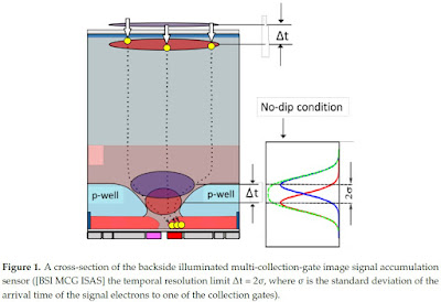
Multi-Collection-Gate 25 Mfps Sensor
MDPI publishes a joint paper by Vietnam National University, Hanoi University of Science and Technology, Imec, Ritsumeikan University, and Kindai University "An Image Signal Accumulation Multi-Collection-Gate Image Sensor Operating at 25 Mfps with 32 × 32 Pixels and 1220 In-Pixel Frame Memory" by Vu Truong Son Dao, Nguyen Ngo, Anh Quang Nguyen, Kazuhiro Morimoto, Kazuhiro Shimonomura, Paul Goetschalckx, Luc Haspeslagh, Piet De Moor, Kohsei Takehara, and Takeharu Goji Etoh.
"The paper presents an ultra-high-speed image sensor for motion pictures of reproducible events emitting very weak light. The sensor is backside-illuminated. Each pixel is equipped with multiple collection gates (MCG) at the center of the front side. Each collection gate is connected to an in-pixel large memory unit, which can accumulate image signals captured by repetitive imaging. The combination of the backside illumination, image signal accumulation, and slow readout from the in-pixel signal storage after an image capturing operation offers a very high sensitivity. Pipeline signal transfer from the the multiple collection gates (MCG) to the in-pixel memory units enables the sensor to achieve a large frame count and a very high frame rate at the same time. A test sensor was fabricated with a pixel count of 32 × 32 pixels. Each pixel is equipped with four collection gates, each connected to a memory unit with 305 elements; thus, with a total frame count of 1220 (305 × 4) frames. The test camera achieved 25 Mfps, while the sensor was designed to operate at 50 Mfps."


"The paper presents an ultra-high-speed image sensor for motion pictures of reproducible events emitting very weak light. The sensor is backside-illuminated. Each pixel is equipped with multiple collection gates (MCG) at the center of the front side. Each collection gate is connected to an in-pixel large memory unit, which can accumulate image signals captured by repetitive imaging. The combination of the backside illumination, image signal accumulation, and slow readout from the in-pixel signal storage after an image capturing operation offers a very high sensitivity. Pipeline signal transfer from the the multiple collection gates (MCG) to the in-pixel memory units enables the sensor to achieve a large frame count and a very high frame rate at the same time. A test sensor was fabricated with a pixel count of 32 × 32 pixels. Each pixel is equipped with four collection gates, each connected to a memory unit with 305 elements; thus, with a total frame count of 1220 (305 × 4) frames. The test camera achieved 25 Mfps, while the sensor was designed to operate at 50 Mfps."


Subscribe to:
Posts (Atom)