Friday, June 30, 2023

Random number generation from image sensor noise

A recent preprint titled "Practical Entropy Accumulation for Random Number Generators with Image Sensor-Based Quantum Noise Sources" by Choi et al. is available here:  https://www.preprints.org/manuscript/202306.1169/v1

 Abstract: The efficient generation of high-quality random numbers is essential in the operation of cryptographic modules. The quality of a random number generator is evaluated by the min-entropy of its entropy source. Typical method used to achieve high min-entropy of the output sequence is an entropy accumulation based on a hash function. This is grounded in the famous Leftover Hash Lemma which guarantees a lower bound on the min-entropy of the output sequence. However, the hash function based entropy accumulation has slow speed in general. For a practical perspective we need a new efficient entropy accumulation with the theoretical background for the min-entropy of the output sequence. In this work, we obtain the theoretical bound for the min-entropy of the output random sequence through the very efficient entropy accumulation using only bitwise XOR operations, where the input sequences from the entropy source are independent. Moreover we examine our theoretical results by applying to the quantum random number generator that uses dark noise arising from image sensor pixels as its entropy source.


Wednesday, June 28, 2023

Image Sensors World Blog Feedback Survey 2023 is open until July 7, 2023

--- Updated Dec 20, 2023 to remove form link ---
 
We would like to know more about our readership and get feedback on how this blog can better serve you.

Please fill the form below (or use this Microsoft Form link: [removed])
 
This survey is completely anonymous; we do not collect any personally identifying information (name, email, etc.)

There are 5 required questions. It won't take more than a few minutes.

Please respond by midnight your local time on July 7, 2023.

Thank you so much for your time!

Coherent - TriEye collaboration on SWIR imaging

PRESS RELEASE

COHERENT AND TRIEYE DEMONSTRATE LASER-ILLUMINATED SHORTWAVE INFRARED IMAGING SYSTEM FOR AUTOMOTIVE AND ROBOTIC APPLICATIONS

PITTSBURGH and TEL AVIV, Israel, June 26, 2023 (GLOBE NEWSWIRE) – Coherent Corp. (NYSE: COHR), a leader in semiconductor lasers, and TriEye Ltd., a pioneer in mass-market shortwave infrared (SWIR) sensing technology, today announced their successful joint demonstration of a laser-illuminated SWIR imaging system for automotive and robotic applications. 

The growing number of use cases for SWIR imaging, which expands vision in automotive and robotics beyond the visible spectrum, is driving demand for low-cost mass-market SWIR cameras. The companies leveraged TriEye’s spectrum enhanced detection and ranging (SEDAR) product platform and Coherent’s SWIR semiconductor laser to jointly design a laser-illuminated SWIR imaging system, the first of its kind that is able to reach lower cost points while achieving very high performance over a wide range of environmental conditions. The combination of these attributes is expected to enable wide deployment in applications such as front and rear cameras in cars as well as vision systems in industrial and autonomous robots. 

“This new solution combines best-in-class SWIR imaging and laser illumination technologies that will enable next-generation cameras to provide images through rain or fog, and in any lighting condition, from broad daylight to total darkness at night,” said Dr. Sanjai Parthasarathi, Chief Marketing Officer at Coherent Corp. “Both technologies are produced leveraging high-volume manufacturing platforms that will enable them to achieve the economies of scale required to penetrate markets in automotive and robotics.”

“We are happy to collaborate with a global leader in semiconductor lasers and to establish an ecosystem that the automotive and industrial robotics industries can rely on to build next-generation solutions,” said Avi Bakal, CEO and co-founder of TriEye. “This is the next step in the evolution of our technology innovation, which will enable mass-market applications. Our collaboration will allow us to continue revolutionizing sensing capabilities and machine vision by allowing the incorporation of SWIR technology into a greater number of emerging applications.”

The SEDAR product platform integrates TriEye’s next-generation CMOS-based SWIR sensor and illumination source with Coherent’s 1375 nm edge-emitting laser on surface-mount technology (SMT). The laser-illuminated imaging systems will enable the next generation of automotive cameras that can provide images through inclement weather. They will also enable autonomous robots to operate around the clock in any lighting conditions and move seamlessly between indoor and outdoor environments.

Coherent and TriEye will exhibit the imaging system at Laser World of Photonics in Munich, Germany, June 27-30, at Coherent’s stand B3.321. 


About TriEye

TriEye is the pioneer of the world’s first CMOS-based Shortwave Infrared (SWIR) image-sensing solutions. Based on advanced academic research, TriEye’s breakthrough technology enables HD SWIR imaging and accurate deterministic 3D sensing in all weather and ambient lighting conditions. The company’s semiconductor and photonics technology enabled the development of the SEDAR (Spectrum Enhanced Detection And Ranging) platform, which allows perception systems to operate and deliver reliable image data and actionable information while reducing expenditure up to 100x the existing industry rates. For more information, visit www.TriEye.tech.


About Coherent

Coherent empowers market innovators to define the future through breakthrough technologies, from materials to systems. We deliver innovations that resonate with our customers in diversified applications for the industrial, communications, electronics, and instrumentation markets. Headquartered in Saxonburg, Pennsylvania, Coherent has research and development, manufacturing, sales, service, and distribution facilities worldwide. For more information, please visit us at coherent.com. 


Contacts

TriEye Ltd.
Nitzan Yosef Presburger
Head of Marketing
news@trieye.tech

Coherent Corp.
Mark Lourie
Vice President, Corporate Communications
corporate.communications@coherent.com 

Monday, June 26, 2023

RADOPT 2023: workshop on radiation effects on optoelectronics and photonics technologies


RADOPT 2023: Workshop on Radiation Effects on      Optoelectronic Detectors and Photonics Technologies

28-30 Nov 2023 Toulouse (France)


First Call for Papers

You are cordially invited to participate to the second edition of the RADECS Workshop on Radiation Effects on Optoelectronics and Photonics Technologies (RADOPT 2023) to be held on 28th-30th November 2023 in Toulouse, France.

After the success of RADOPT 2021, this second edition of the workshop, will continue to combine and replace two well-known events from the Photonic Devices and IC’s community: the “Optical Fibers in Radiation Environments Days -FMR and the Radiation effects on Optoelectronic Detectors Workshop, traditionally organized every-two years by the COMET OOE of CNES.

The objective of the workshop is to provide a forum for the presentation and discussion of recent developments regarding the use of optoelectronics and photonics technologies in radiation-rich environments The workshop also offers the opportunity to highlight future prospects in the fast-moving space, high energy physics, fusion and fission research fields and to enhance exchanges and collaborations between scientists. Participation of young researchers (PhD) is especially encouraged.
Oral and poster communications are solicited reporting on original research (both experimental and theoretical) in the following areas:

  • Basic Mechanisms of radiation effects on optical properties of materials, devices and systems
  • Silicon Photonics, Photonic Integrated Circuits
  • Solar Cells
  • Cameras, Image sensors and detectors
  • Optically based dosimetry and beam monitoring techniques
  • Fiber optics and fiber-based sensors
  • Optoelectronics components and systems

Abstract Submission and Decision Notification:

Abstracts for both oral and poster presentations can be submitted. The final decision will be taken by the RADOPT Scientific Committee.

·       Abstract submission open: Monday April 3rd, 2023

·       Abstract submission deadline: Friday July 9th, 2023

à Send abstract to clementine.durnez@cnes.fr

Industrial Exhibition

An industrial exhibition will be organized during RADOPT 2023. The location allows the exhibits to be located adjacent to the auditorium where the oral sessions will be delivered. Please contact us for more details.


Friday, June 23, 2023

Canon presentation on CIS PPA Optimization

Canon presentation on "PPA Optimization Using Cadence Cerebrus for CMOS Image Sensor Designs" is available here: https://vimeo.com/822031091

Some slides:


Wednesday, June 21, 2023

ICCP Program Available, Early Registration Ends June 22

The IEEE International Conference on Computational Photography (ICCP) program is now available online: https://iccp2023.iccp-conference.org/conference-program/

ICCP is an in-person conference to be held at the Monona Terrace Conventional Center in Madison, WI (USA) from July 28-30, 2023.

Early registration ends June 22: https://iccp2023.iccp-conference.org/registration/

Friday, July 28th

09:00 Opening Remarks

09:30 Session 1: Polarization and HDR Imaging
1) Learnable Polarization-multiplexed Modulation Imager for Depth from Defocus
2) Polarization Multi-Image Synthesis with Birefringent Metasurfaces
3) Glare Removal for Astronomical Images with High Local Dynamic Range
4) Polarimetric Imaging Spaceborne Calibration Using Zodiacal Light

10:30 Invited Talk: Melissa Skala (UW-Madison)
Unraveling Immune Cell Metabolism and Function at Single-cell Resolution

11:00 Coffee break

11:30 Keynote: Aki Roberge (NASA)
Towards Earth 2.0: Exoplanets and Future Space Telescopes

12:30 Lunch; Industry Consortium Mentorship Event

14:00 Invited Talk: Lei Li (Rice)
New Generation Photoacoustic Imaging: From Benchtop Wholebody Imagers to Wearable Sensors

14:30 Session 2: Emerging and Unconventional Computational Sensing
1) CoIR: Compressive Implicit Radar
2) Parallax-Driven Denoising of Passively-Scattered Thermal Imagery
3) Moiré vision: A signal processing technology beyond pixels using the Moiré coordinate

15:15 Poster and demo Spotlights

15:30 Coffee break

16:00 Poster and demo Session 1

17:30 Community Poster and Demo Session


Saturday, July 29th

09:00 Invited Talk: Ellen Zhong (Princeton)
Machine Learning for Determining Protein Structure and Dynamics from Cryo-EM Images

09:30 Session 3: Neural and Generative Methods in Imaging
1) Learn to Synthesize Photorealistic Dual-pixel Images from RGBD frames
2) Denoising Diffusion Probabilistic Model for Retinal Image Generation and Segmentation
3) NeReF: Neural Refractive Field for Fluid Surface Reconstruction and Rendering
4) Supervision by Denoising

10:30 Invited Talk: Karen Schloss (UW-Madison)

11:00 Coffee break

11:30 Keynote: Aaron Hertzmann (Adobe)
A Perceptual Theory of Perspective

12:30 Lunch; Affinity Group Meetings

14:00 Invited Talk: Na Ji (UC Berkeley)

14:30 Session 4: Measuring Spectrum and Reflectance
1) Spectral Sensitivity Estimation Without a Camera
2) A Compact BRDF Scanner with Multi-conjugate Optics
3) Measured Albedo in the Wild: Filling the Gap in Intrinsics Evaluation
4) Compact Self-adaptive Coding for Spectral Compressive Sensing

15:30 Industry Consortium Talk: Tomoo Mitsunaga (Sony)
Computational Image Sensing at Sony

16:00 Poster and Demo Spotlights

16:15 Coffee Break

16:45 Poster and Demo Session 2

18:15 Reception


Sunday, July 30th

09:00 Session 5: Depth and 3D Imaging
1) Near-light Photometric Stereo with Symmetric Lights
2) Aberration-Aware Depth-from-Focus
3) Count-Free Single-Photon 3D Imaging with Race Logic

09:45 Invited Talk: Jules Jaffe (Scripps & UCSD)
Welcome to the Underwater Micro World: The Art and Science of Underwater Microscopy

10:15 Coffee Break

10:45 Invited Talk: Hooman Mohseini (Northwestern University)
New Material and Devices for Imaging

11:15 Keynote: Eric Fossum (Dartmouth)
Quanta Image Sensors and Remaining Challenges

12:15 Lunch; Industry Consortium Mentorship Event

12:45 Lunch (served)

14:00 Session 6: NLOS Imaging and Imaging Through Scattering Media
1) Isolating Signals in Passive Non-Line-of-Sight Imaging using Spectral Content
2) Fast Non-line-of-sight Imaging with Non-planar Relay Surfaces
3) Neural Reconstruction through Scattering Media with Forward and Backward Losses

14:45 Invited Talk: Jasper Tan (Glass Imaging)
Towards the Next Generation of Smartphone Cameras

15:15 Session 7: Holography and Phase-based Imaging
1) Programmable Spectral Filter Arrays using Phase Spatial Light Modulators
2) Scattering-aware Holographic PIV with Physics-based Motion Priors
3) Stochastic Light Field Holography

16:00 Closing Remarks

NEC uncooled IR camera uses carbon nanotubes

From JCN Newswire: https://www.jcnnewswire.com/english/pressrelease/82919/3/NEC-develops-the-world&aposs-first-highly-sensitive-uncooled-infrared-image-sensor-utilizing-carbon-

NEC develops the world's first highly sensitive uncooled infrared image sensor utilizing carbon nanotubes

- More than three times the sensitivity of conventional uncooled infrared image sensors -
TOKYO, Apr 10, 2023 - (JCN Newswire) - NEC Corporation (TSE: 6701) has succeeded in developing the world's first high-sensitivity uncooled infrared image sensor that uses high-purity semiconducting carbon nanotubes (CNTs) in the infrared detection area. This was accomplished using NEC's proprietary extraction technology. NEC will work toward the practical application of this image sensor in 2025.

Infrared image sensors convert infrared rays into electrical signals to acquire necessary information, and can detect infrared rays emitted from people and objects even in the dark. Therefore, infrared image sensors are utilized in various fields to provide a safe and secure social infrastructure, such as night vision to support automobiles driving in the darkness, aircraft navigation support systems and security cameras.

There are two types of infrared image sensors, the "cooled type," which operates at extremely low temperatures, and the "uncooled type," which operates near room temperature. The cooled type is highly sensitive and responsive, but requires a cooler, which is large, expensive, consumes a great deal of electricity, and requires regular maintenance. On the other hand, the uncooled type does not require a cooler, enabling it to be compact, inexpensive, and to consume low power, but it has the issues of inferior sensitivity and resolution compared to the cooled type.


In 1991, NEC discovered CNTs for the first time in the world and is now a leader in research and development related to nanotechnology. In 2018, NEC developed a proprietary technology to extract only semiconducting-type CNTs at high purity from single-walled CNTs that have a mixture of metallic and semiconducting types. NEC then discovered that thin films of semiconducting-type CNTs extracted with this technology have a large temperature coefficient of resistance (TCR) near room temperature.

The newly developed infrared image sensor is the result of these achievements and know-how. NEC applied semiconductor-type CNTs based on its proprietary technology that features a high TCR, which is an important index for high sensitivity. As a result, the new sensor achieves more than three times higher sensitivity than mainstream uncooled infrared image sensors using vanadium oxide or amorphous silicon.

The new device structure was achieved by combining the thermal separation structure used in uncooled infrared image sensors, the Micro Electro Mechanical Systems (MEMS) device technology used to realize this structure, and the CNT printing and manufacturing technology cultivated over many years for printed transistors, etc. As a result, NEC has succeeded in operating a high-definition uncooled infrared image sensor of 640 x 480 pixels by arraying the components of the structure.

Part of this work was done in collaboration with Japan's National Institute of Advanced Industrial Science and Technology (AIST). In addition, a part of this achievement was supported by JPJ004596, a security technology research promotion program conducted by Japan's Acquisition, Technology & Logistics Agency (ATLA).

Going forward, NEC will continue its research and development to further advance infrared image sensor technologies and to realize products and services that can contribute to various fields and areas of society.


Tuesday, June 20, 2023

Webinar on Latest Trends in High-speed Imaging & Introduction to BSI Sensors

Webinar on latest trends in High-Speed Camera, Introducing the BSI Camera Sensor.

Join this free tech talk by our expert speakers of Phantom High-Speed Cameras - Vision Research in which we explore the latest trends in high-speed cameras focusing on Backside Illuminated (BSI) sensor cameras and the associated benefits of improved processing speed and fill factor along with the challenges in such high-speed designs.

Webinar registration [link]

Date: 22nd June 2023
Time: 2:30pm IST / 2:00am Pacific / 5:00am Eastern

Topics to be covered:
Introducing the BSI sensor camera
Introducing FORZA & Sensor Insights
Introducing the MIRO C camera
Demo & display of the High-Speed Camera & its accessories.


Monday, June 19, 2023

A lens-less and sensor-less camera

An interesting combination of tech+art: https://bjoernkarmann.dk/project/paragraphica 

Paragraphica is a context-to-image camera that uses location data and artificial intelligence to visualize a "photo" of a specific place and moment. The camera exists both as a physical prototype and a virtual camera that you can try.


Will this put the camera and image sensor industry out of business? :)


Friday, June 16, 2023

Videos du jour --- Sony, onsemi, realme/Samsung [June 16, 2023]


Stacked CMOS Image Sensor Technology with 2-Layer Transistor Pixel | Sony Official

Sony Semiconductor Solutions Corporation (“SSS”) has succeeded in developing the world’s first* stacked CMOS image sensor technology with 2-Layer Transistor Pixel.
This new technology will prevent underexposure and overexposure in settings with a combination of bright and dim illumination (e.g., backlit settings) and enable high-quality, low-noise images even in low-light (e.g., indoor, nighttime) settings.
LYTIA image sensors are designed to enable smartphone users to express and share their emotions more freely and to bring a creative experience far beyond your imagination. SSS continues to create a future where everyone can enjoy a life full of creativity with LYTIA.
*: As of announcement on December 16, 2021.


New onsemi Hyperlux Image Sensor Family Leads the Way in Next-Generation ADAS to Make Cars Safer
onsemi's new Hyperlux™ image sensors are steering the future of autonomous driving!
Armed with 150db ultra-high dynamic range to capture high-quality images in the most extreme lighting conditions, our Hyperlux™ sensors use up to 30% less power with a footprint that's up to 28% smaller than competing devices.


When realme11Pro+ gets booted with ISOCELL HP3 Super Zoom, a 200MP Image Sensor | realme
The ISOCELL HP3 SuperZoom, a 200MP image sensor, equipped in realme 11 Pro+ combined with realme’s advanced camera technology. What will you capture with this innovation?


Thursday, June 15, 2023

Sony’s World-first two-layer image sensor: TechInsights preliminary analysis and results

By TechInsights Image Sensor Experts: Eric Rutulis, John Scott-Thomas, PhD

We first heard about it at IEDM 2021, and Sony provided more details at the 2022 IEEE Symposium on VLSI Technology and Circuits conference. Now it’s on the market and TechInsights has had our first look at the “world’s first” two-layer image sensor and we present our preliminary results here. The device was found in a Sony Xperia 1V smartphone main camera having a 48 MP, 1.12 µm pixel pitch and we can confirm it has dual photodiodes (a Left and Right photodiode in each pixel for full array PDAF). The die size measures 11.37 x 7.69 mm edge-to-edge.

In fact, the sensor actually has three layers of active silicon, with an Image Signal Processor (ISP) stacked in a conventional arrangement using a Direct Bond Interface (DBI) to the “second layer” (we will use Sony’s nomenclature when possible) of the CMOS Image Sensor (CIS). Figure 1 shows a SEM cross-section through the array. Light enters from the bottom of the image, through the microlenses and color filters. Each pixel is separated by an aperture grid (with compound layers) to increase the quantum efficiency. Front Deep Trench Isolation is used between each photodiode and it appears that Sony is using silicon dioxide in the deep trench to improve Full Well Capacity and Quantum Efficiency (this will be confirmed with further analysis).This layer also has the planar Transfer Gate used to transfer photocharge from the diode to the floating diffusion. Above the first layer is the “second layer” of silicon that contains three transistors for each pixel; the Reset, Amp (Source-Follower) and Select transistors. These transistors sit above the second layer silicon and connection to the first layer is achieved using “Deep contacts” which pass through the second layer essentially forming Through Silicon Vias (TSVs). Finally, the ISP sits above the metallization of the second layer, connected using Hybrid (Direct) Bonding. The copper of the ISP used for connection to the CIS DBI Cu is not visible in this image.

Figure 1: SEM Cross-section through the sensor indicating the three active silicon layers.

Key to this structure is a process flow that can withstand the thermal cycling needed to create the thermal oxide and activate the implants on the second layer. Sony has described the process flow in some detail (IEDM 2021, “3D Sequential Process Integration for CMOS Image Sensor”).

Figure 2 is an image from this paper showing the process flow. The first layer photodiodes and Transfer Gate are formed, and the second layer is wafer bonded and thinned. Only then are the second layer gate oxides formed and the implants are activated. Finally, the deep contacts are formed, etching through the second layer, and contacting the first layer devices.

Figure 2: Process flow for two-layer CIS described in “3D Sequential Process Integration for CMOS Image Sensor”, IEDM 2021.


The interface between the first and second layer is shown in more detail in Figure 3. The Transfer Gate (TG in the image) is connected to the first metal layer of the second layer. Slightly longer deep contacts lie below the sample surface and are partially visible in the image. These connect the floating diffusion node between the first and second layer. A sublocal connection (below the sample surface) is used to interconnect four photodiodes just above the first layer to the source of the Reset FET and gate of the AMP (Source-Follower) FET.

 
                    Figure 3: SEM cross-section detail of the first and second layer interface.

The sublocal connection is explored more in Figure 4. This is a planar SEM image of the first layer at the substrate level. Yellow boxes outline the pixel, with PDL and PDR indicating the left and right photodiodes. One microlense covers each pixel. Sublocal connections are indicated and are used to interconnect the Floating Diffusion for two pixels and ground for four pixels. The sublocal connection appears to be polysilicon; this is currently being confirmed with further analysis.


Figure 4: SEM planar view of the pixel first layer at the substrate level.


The motivation for the two-layer structure is multiple. The photodiode full well capacity can be maintained even with the reduced pixel pitch. The use of sublocal contacts reduces the capacitance of the floating diffusion, increasing the conversion gain of the pixels. The increased area available on the second layer allows the AMP (Source-Follower) transistor area to be increased, reducing noise (flicker and telegraph) create in the channel of this device.

It's worth taking a moment to appreciate Sony’s achievement here. The new process flow and deep contact technology allow two layers of active devices to be interconnected with an impressive 0.46 µm (center-to-center) spacing of the deep contacts (or Through Silicon Vias). Even the hybrid bonding to the ISP is just 1.12 µm; the smallest pitch TechInsights has seen to date. At the recent International Image Sensors Workshop, Sony described an upcoming generation that will use “buried” sublocal connections embedded in the first layer and pixel FinFets in the second layer (to be published). Perhaps we are seeing the first stages of truly three-dimensional circuitry, with active devices on multiple layers of silicon, all interconnected. Congratulations, Sony!

TechInsights' first Device Essentials analysis on this device will be published shortly with more analyses underway.

Access the TechInsights Platform for more content and reports on image sensors.


Wednesday, June 14, 2023

inVISION Days Conference presentations

inVISION Days Conference presentations are now available online.

The first day of the inVISION Days Conference will give an overview of current developments in cameras and lenses, such as new image sensors for applications outside the visible range, high-speed interfaces... The panel discussion will explore what to expect next in image sensors.

All webinars are available for free (create a login account first):
https://openwebinarworld.com/en/webinar/invision-days-day-1-cameras/#video_library
 

Session 1: Machine Vision Cameras
Session 2: Optics & Lenses
Session 3: High-Speed Vision


At the first inVISION Day Metrology current applications and new technologies will be presented at the four sessions 3D Scanner, Inline Metrology, Surface Metrology, CT & X-Ray. The free online conference will be completed by a keynote speech, the panel discussion 'Metrology in the Digital Age' and the EMVA Pitches, where four start-up companies will present their innovations. You can find more information under invdays.com/metrology.

https://openwebinarworld.com/en/webinar/invision-day-metrology/
 
Session 1: 3D Scanner
Session 2: Inline Metrology
Session 3: Surface Metrology
Session 4: CT & X-ray

Tuesday, June 13, 2023

PetaPixel article on an 18K (316MP) HDR sensor

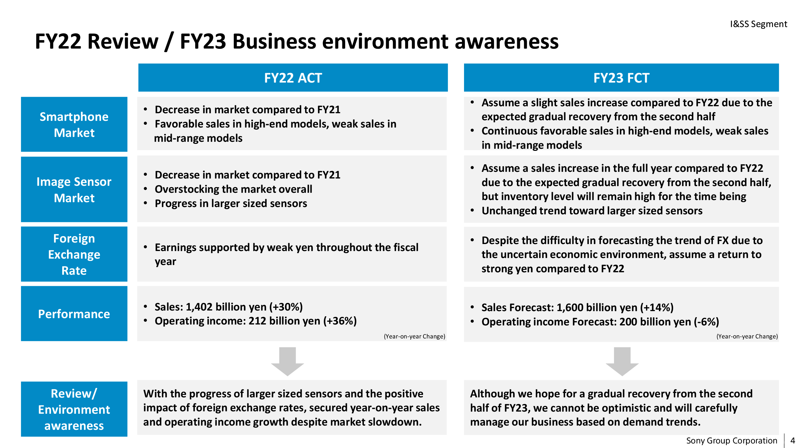
Link: https://petapixel.com/2023/06/12/sphere-studios-big-sky-cinema-camera-features-an-insane-18k-sensor/

Sphere Studios’ Big Sky Cinema Camera Features an Insane 18K Sensor

Sphere Studios has developed a brand new type of cinema camera called The Big Sky. It features a single 316-megapixel HDR image sensor that the company says is a 40x resolution increase over existing 4K cameras and PetaPixel was given an exclusive look at the incredible technology.


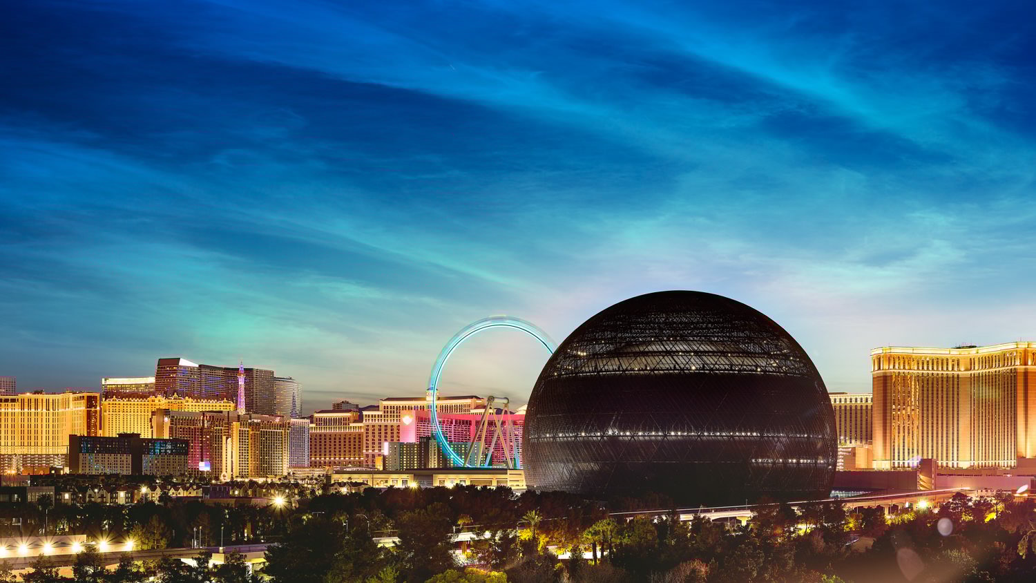
Those who have visited Las Vegas in the last few years may have noticed the construction of a giant sphere building near the Venetian Hotel. Set to open in the fall of 2023, the Sphere Entertainment Co has boasted that this new facility will provide “immersive experiences at an unparalleled scale” featuring a 580,000 square-foot LED display and the largest LED screen on Earth.

As PetaPixel covered last fall, the venue will house the world’s highest resolution LED screen: a 160,000 square-foot display plane that will wrap up, over, and behind the audience at a resolution over 80 times that of a high-definition television with approximately 17,500 seats and a scalable capacity up to 20,000 guests. While the facility for viewing these immersive experiences sounds impressive on its own, it leaves one wondering what kind of cameras and equipment are needed to capture the content that gets played there.

The company has said “an innovative new camera system developed internally that sets a new bar for Image fidelity, eclipsing all current cinematic cameras with unparalleled edge-to-edge sharpness” — a very bold claim. While on paper it doesn’t seem much different from any other camera manufactures claims about their next-gen system, spending time with the new system in person and seeing what it is capable of paints an entirely different picture that honestly has to be seen to be believed.

“Sphere Studios is not only creating content, but also technology that is truly transformative,” says David Dibble, Chief Executive Officer of MSG Ventures, a division of Sphere Entertainment focused on developing advanced technologies for live entertainment.

“Sphere in Las Vegas is an experiential medium featuring an LED display, sound system and 4D technologies that require a completely new and innovative approach to filmmaking. We created Big Sky – the most advanced camera system in the world – not only because we could, but out of innovative necessity. This was the only way we could bring to life the vision of our filmmakers, artists, and collaborators for Sphere.”

According to the company, the new Big Sky camera system “is a groundbreaking ultra-high-resolution camera system and custom content creation tool that was developed in-house at Sphere Studios to capture stunning video for the world’s highest resolution screen at Sphere. Every aspect of Big Sky represents a significant advancement on current state-of-the-art cinema camera systems, including the largest single sensor in commercial use capable of capturing incredibly detailed, large-format images.”

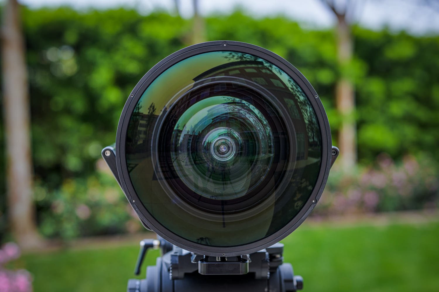
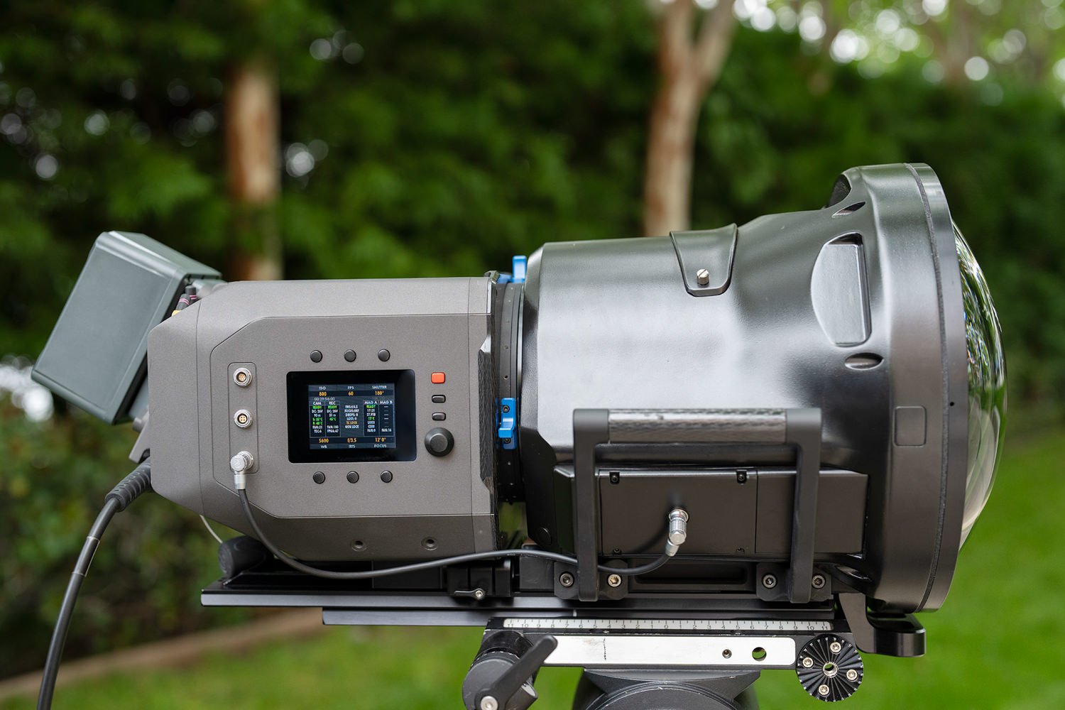
The Big Sky features an “18K by 18K” (or 18K Square Format) custom image sensor which absolutely dwarfs current full frame and large format systems. When paired with the Big Sky’s single-lens system –which the company boasts is the world’s sharpest cinematic lens — it can achieve the extreme optical requirements necessary to match Sphere’s 16K by 16K immersive display plane from edge to edge.

Currently the camera has two primary lens designs: a 150-degree field of view which is true to the view of the sphere where the content will be projected, and a 165-degree field of view which is designed for “overshoot and stabilization” particularly useful in filming situations where the camera is in rapid motion or on an aircraft with a lot of vibrations (ie a helicopter).

The Big Sky features a single 316-megapixel, 3-inch by 3-inch HDR image sensor that the company says is a 40x resolution increase over existing 4K cameras and 160x over HD cameras. In addition to its massive sensor size, the camera is capable of capturing 10-bit footage at 120 frames per second (FPS) in the 18K square format as well as 60 FPS at 12-bit.

“With underwater and other lenses currently in development, as well as the ability to use existing medium format lenses, Sphere Studios is giving immersive content creators all the tools necessary to create extraordinary content for Sphere,” the company says.

Since the media captured by the Big Sky camera is massive, it requires some substantial processing power as well as some objectively obscene amounts of storage solutions. As such, just like the lenses, housings (including underwater and aerial gimbals), and camera, the entire media recorder infrastructure was designed and built entirely in-house to precisely meet the company’s needs.

According to the engineering team at Sphere, “the Big Sky camera creates a 500 gigabit per second pipe off the camera with 400 gigabit of fiber between the camera head and the media recorder. The media recorder itself is currently capable of recording 30 gigabytes of data per second (sustained) with each media magazine containing 32 terabytes and holds approximately 17 minutes of footage.”
The company says the media recorder is capable of handling 600 gigabits per second of network connectivity, as well as built-in media duplication, to accelerate and simplify on-set and post-production workflows. This allows their creative team to swap out drives and continue shooting for as long as they need.

Basically, as long as they have power and extra media magazines, they can run the camera pretty much all day without any issues. I did ask the team about overheating and heat dissipation of the massive system, and they went into great detail about how the entire system has been designed with a sort of internal “chimney” that maintained airflow through the camera ensuring it would not overheat and can keep running even in some of the craziest weather scenarios ranging from being completely underwater to surrounded by dust storms without incident.

What’s even more impressive is the camera can run completely separate from this recording technology as long as it is connected through its cable system, this includes distances of up to a reported mile away.

Since the entire system was built in-house, the team at Sphere Studios had to build their own image processing software specifically for Big Sky that utilizes GPU-accelerated RAW processing to make the workflows of capturing and delivering the content to the Sphere screen practical and efficient. Through the use of proxy editing, a standard laptop can be used, connected to the custom media decks to view and edit the footage with practically zero lag.

Why Is This A Big Deal?
While the specs on paper are unarguably mind-boggling, it’s practically impossible to express just how impressive the footage and experience is to see it captured and presented on the sphere screens it was meant for.

The good news is that PetaPixel was invited to the Los Angeles division for a private tour and demonstration of the groundbreaking technology so we could see it all firsthand and not just go off of the press release. I wasn’t able to take photos or video myself — the images and video in this write-up were provided by the Sphere Studios team — but I can confirm that this technology is wildly impressive and will definitely change the filmmaking industry in the coming years.

When showing me the initial concepts and design mock-ups, the team didn’t think of the content they deliver as simply footage, but rather “experiential storytelling” and after having experienced it for myself, I wholeheartedly agree.

During my tour of the facility, I got to see the camera first hand, look at live footage and rendering in real-time, as well as see some test images and video footage, including some scenes that may make it into “Postcard from Earth” which is the first experience being revealed at the Sphere in Las Vegas this fall that has footage captured from all over the planet that should give viewers a truly unique perspective of what the planet and this new camera system has to offer.

On top of the absolutely massive camera, the system they have developed to “experience” the footage includes haptic seating, true personal-headphone level sound without the headphones from any seat, as well as a revolutionary “environmental” system that can help viewers truly feel the environment they are watching with changing temperatures, familiar scents, and even a cool breeze.
“Sphere Studios is not only creating content, but also technology that is truly transformative,” says Dibble.

“Sphere in Las Vegas is an experiential medium featuring an LED display, sound system and 4D technologies that require a completely new and innovative approach to filmmaking. We created Big Sky – the most advanced camera system in the world – not only because we could, but out of innovative necessity. This was the only way we could bring to life the vision of our filmmakers, artists, and collaborators for Sphere.”

Something worth noting is all of this came to life effectively in just a few short years. The camera started out as an “array” of existing 8K cameras mounted in a massive custom housing. This created an entirely new series of challenges when processing and rendering the massive visuals, which lead to the development of the Big Sky single-lens camera itself, which is currently in its version 2.5 stage of development.

Each generation has made the system more compact and efficient also. The original system was over 100 pounds with the current (v2) weighing a little over 60 pounds, with the next generation lens being developed bringing the system under 30 pounds.

Equally impressive was the amount of noise the camera made, which is to say it was practically silent in operation. Even with the cooling system running it was as quiet or even quieter than most existing 8K systems in the cinematic world — comparing it to an IMAX wouldn’t even be fair… to the IMAX.

The Big Sky cameras are not up for sale (yet) but they are meeting with film companies and filmmakers to find ways to bring the technology to the home-entertainment world. A discussion we had on-site revolved around gimbals mounted on helicopters, airplanes, and automobiles and how those systems, even “the best” still experience some jitter/vibration which is often stabilized which causes the footage to be cropped in.


The technology built for Big Sky helps eliminate a massive percentage of this vibration, and even without it, the sheer amount of resolution the camera offers can provide a ton of space for post-production stabilization. This alone could be a game changer for Hollywood when capturing aerial and “chase scene” footage from vehicles allowing for even more detail than ever before.

Big Sky’s premiere experience at Sphere in Las Vegas is set to open on September 29 with the first of 25 concerts by U2, as well as many other film and live event projects that will be announced soon.

Monday, June 12, 2023

Sony Business Segment meeting discusses ambitious expansion plan

Sony held its 2023 Business Segment meeting on May 24, 2023.
https://www.sony.com/en/SonyInfo/IR/library/presen/business_segment_meeting/
 

Slides from its image sensors division below. Sony has quite ambitious plans to touch 85% of the automotive vision sensing market (slide 10).
https://www.sony.com/en/SonyInfo/IR/library/presen/business_segment_meeting/pdf/2023/ISS_E.pdf