Thursday, November 30, 2023

ISSCC 2024 Advanced Program Now Available

ISSCC will be held Feb 18-22, 2024 in San Francisco, CA.

Link to advanced program: https://submissions.mirasmart.com/ISSCC2024/PDF/ISSCC2024AdvanceProgram.pdf

There are several papers of interest in Session 6 on Imagers and Ultrasound. 

6.1 12Mb/s 4×4 Ultrasound MIMO Relay with Wireless Power and Communication for Neural Interfaces
E. So, A. Arbabian (Stanford University, Stanford, CA)

6.2 An Ultrasound-Powering TX with a Global Charge-Redistribution Adiabatic Drive Achieving 69% Power Reduction and 53° Maximum Beam Steering Angle for Implantable Applications
M. Gourdouparis1,2, C. Shi1 , Y. He1 , S. Stanzione1 , R. Ukropec3 , P. Gijsenbergh3 , V. Rochus3 , N. Van Helleputte3 , W. Serdijn2 , Y-H. Liu1,2
 1 imec, Eindhoven, The Netherlands
 2 Delft University of Technology, Delft, The Netherlands
 3 imec, Leuven, Belgium

6.3 Imager with In-Sensor Event Detection and Morphological Transformations with 2.9pJ/pixel×frame Object Segmentation FOM for Always-On Surveillance in 40nm
 J. Vohra, A. Gupta, M. Alioto, National University of Singapore, Singapore, Singapore

6.4 A Resonant High-Voltage Pulser for Battery-Powered Ultrasound Devices
 I. Bellouki1 , N. Rozsa1 , Z-Y. Chang1 , Z. Chen1 , M. Tan1,2, M. Pertijs1
 1 Delft University of Technology, Delft, The Netherlands
 2 SonoSilicon, Hangzhou, China

6.5 A 0.5°-Resolution Hybrid Dual-Band Ultrasound Imaging SoC for UAV Applications
 J. Guo1 , J. Feng1 , S. Chen1 , L. Wu1 , C-W. Tsai1,2, Y. Huang1 , B. Lin1 , J. Yoo1,2
 1 National University of Singapore, Singapore, Singapore
 2 The N.1 Institute for Health, Singapore, Singapore

6.6 A 10,000 Inference/s Vision Chip with SPAD Imaging and Reconfigurable Intelligent Spike-Based Vision Processor
 X. Yang*1 , F. Lei*1 , N. Tian*1 , C. Shi2 , Z. Wang1 , S. Yu1 , R. Dou1 , P. Feng1 , N. Qi1 , J. Liu1 , N. Wu1 , L. Liu1
 1 Chinese Academy of Sciences, Beijing, China 2 Chongqing University, Chongqing, China
 *Equally Credited Authors (ECAs)

6.7 A 160×120 Flash LiDAR Sensor with Fully Analog-Assisted In-Pixel Histogramming TDC Based on Self-Referenced SAR ADC
 S-H. Han1 , S. Park1 , J-H. Chun2,3, J. Choi2,3, S-J. Kim1
 1 Ulsan National Institute of Science and Technology, Ulsan, Korea
 2 Sungkyunkwan University, Suwon, Korea
 3 SolidVue, Seongnam, Korea

6.8 A 256×192-Pixel 30fps Automotive Direct Time-of-Flight LiDAR Using 8× Current-Integrating-Based TIA, Hybrid Pulse Position/Width Converter, and Intensity/CNN-Guided 3D Inpainting
 C. Zou1 , Y. Ou1 , Y. Zhu1 , R. P. Martins1,2, C-H. Chan1 , M. Zhang1
 1 University of Macau, Macau, China
 2 Instituto Superior Tecnico/University of Lisboa, Lisbon, Portugal

6.9 A 0.35V 0.367TOPS/W Image Sensor with 3-Layer Optical-Electronic Hybrid Convolutional Neural Network
 X. Wang*, Z. Huang*, T. Liu, W. Shi, H. Chen, M. Zhang
 Tsinghua University, Beijing, China
 *Equally Credited Authors (ECAs)

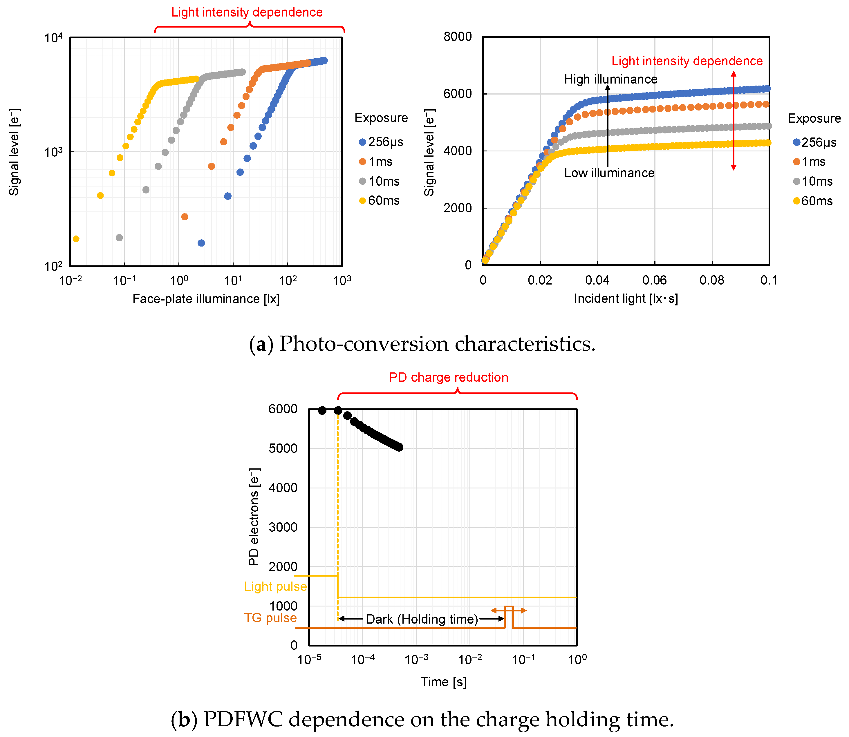
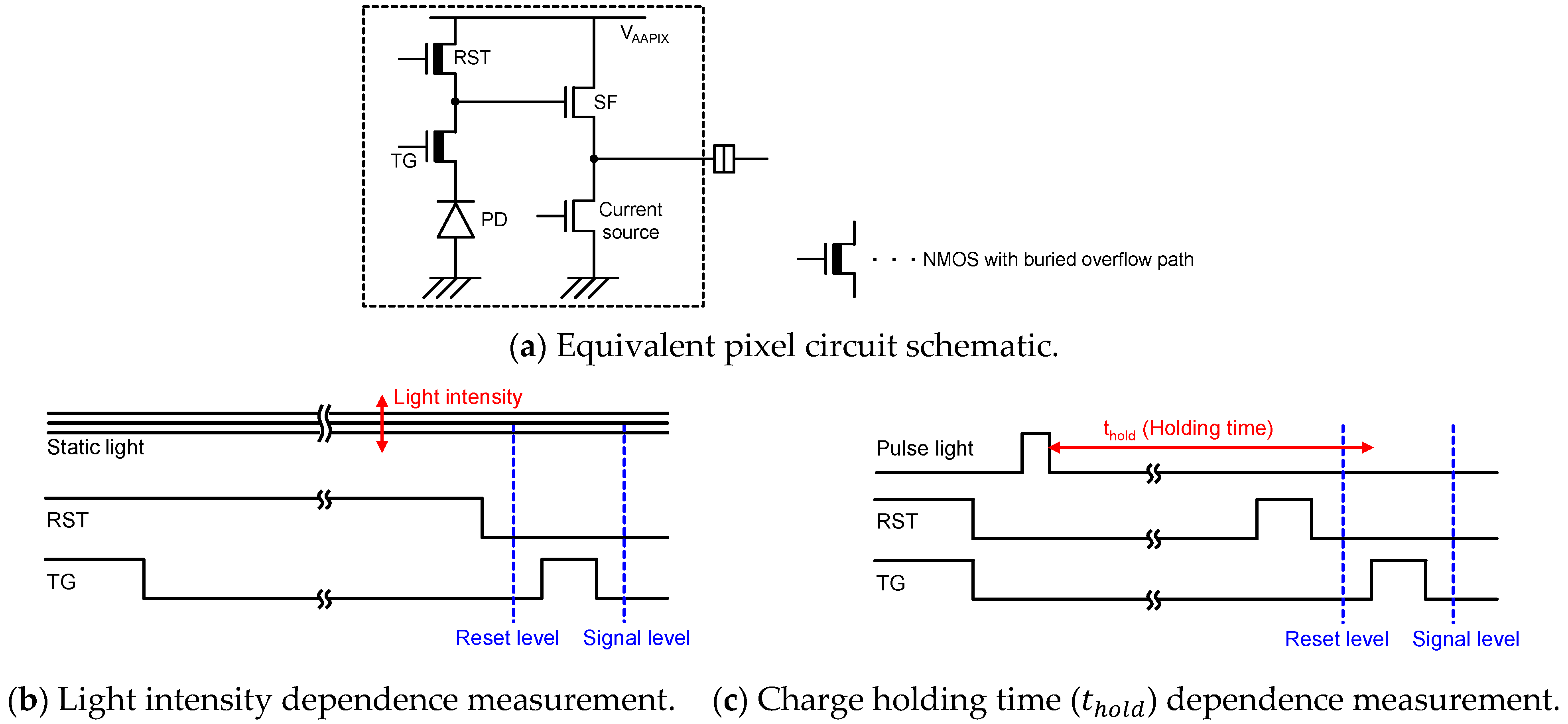
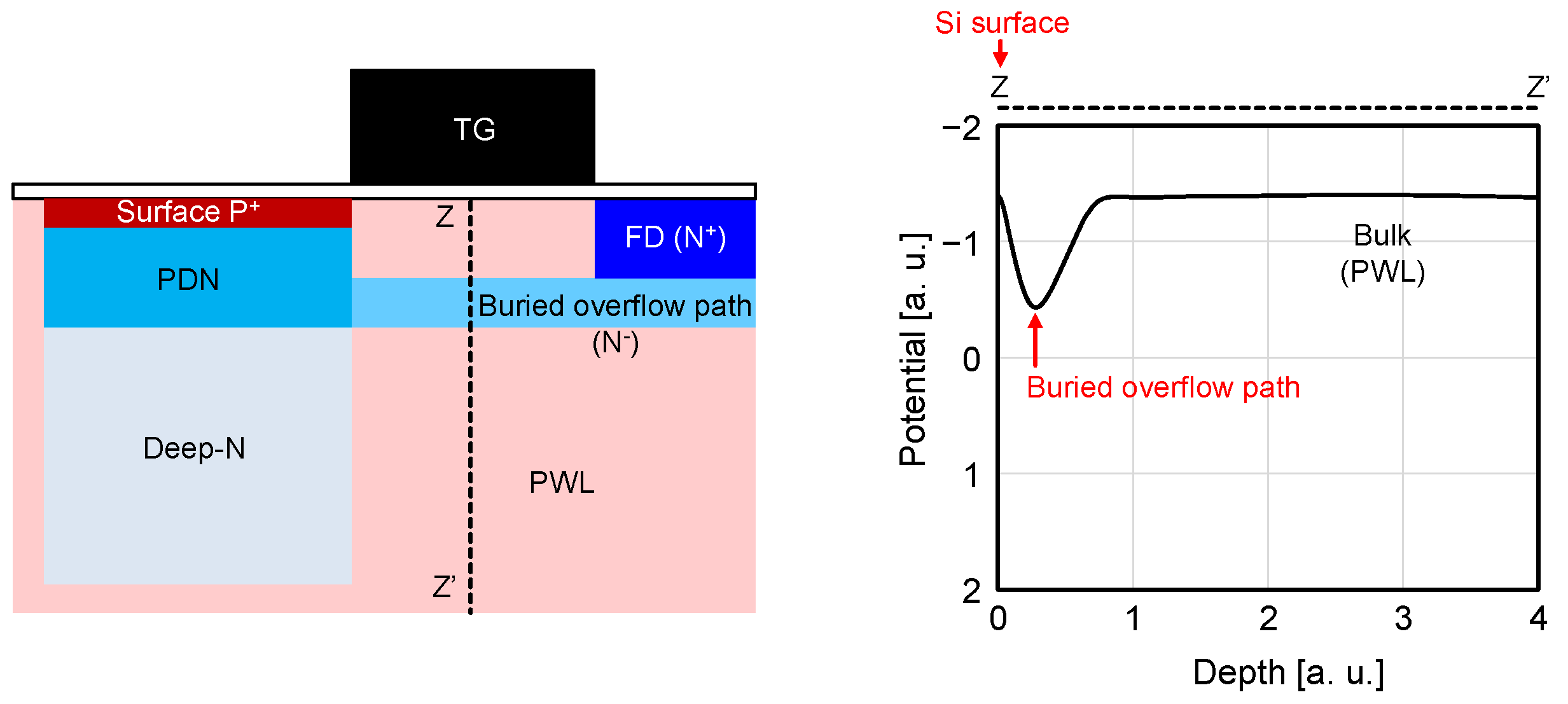
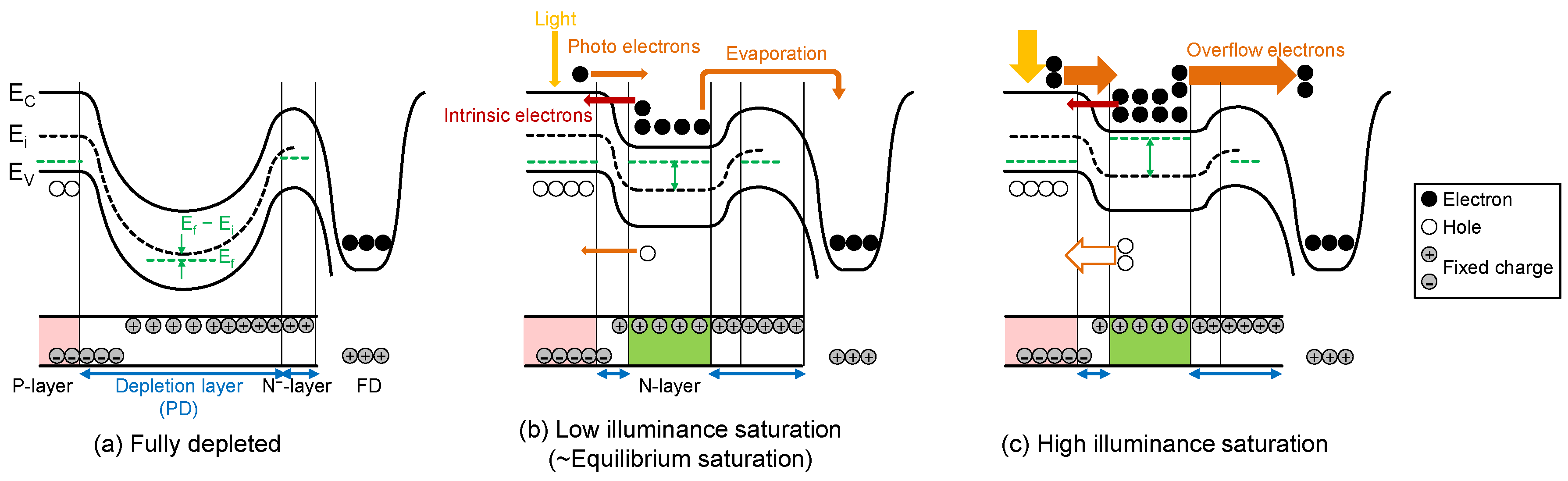
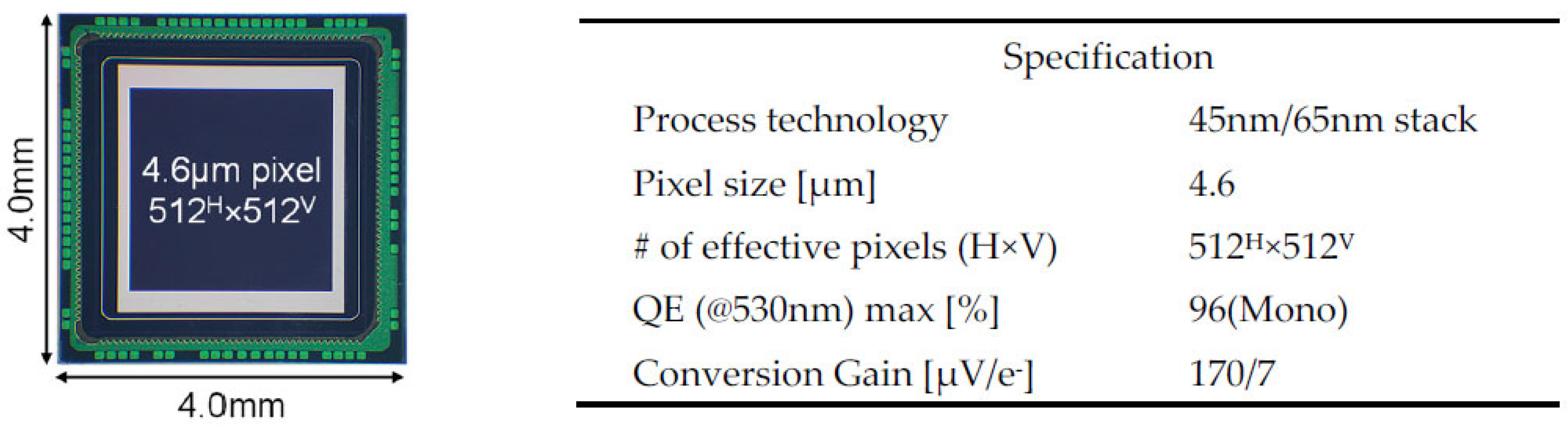
6.10 A 1/1.56-inch 50Mpixel CMOS Image Sensor with 0.5μm pitch Quad Photodiode Separated by Front Deep Trench Isolation
 D. Kim, K. Cho, H-C. Ji, M. Kim, J. Kim, T. Kim, S. Seo, D. Im, Y-N. Lee, J. Choi, S. Yoon, I. Noh, J. Kim, K. J. Lee, H. Jung, J. Shin, H. Hur, K. E. Chang, I. Cho, K. Woo, B. S. Moon, J. Kim, Y. Ahn, D. Sim, S. Park, W. Lee, K. Kim, C. K. Chang, H. Yoon, J. Kim, S-I. Kim, H. Kim, C-R. Moon, J. Song
 Samsung Semiconductor, Hwaseong, Korea

6.11 A 320x240 CMOS LiDAR Sensor with 6-Transistor nMOS-Only SPAD Analog Front-End and Area-Efficient Priority Histogram Memory
 M. Kim*1 , H. Seo*1,2, S. Kim1 , J-H. Chun1,2, S-J. Kim3 , J. Choi*1,2
 1 Sungkyunkwan University, Suwon, Korea
 2 SolidVue, Seongnam, Korea
 3 Ulsan National Institute of Science and Technology, Ulsan, Korea
 *Equally Credited Authors (ECAs)
 

Imaging papers in other sessions: 

17.3 A Fully Wireless, Miniaturized, Multicolor Fluorescence Image Sensor Implant for Real-Time Monitoring in Cancer Therapy
 R. Rabbani*1 , M. Roschelle*1 , S. Gweon1 , R. Kumar1 , A. Vercruysse1 , N. W. Cho2 , M. H. Spitzer2 , A. M. Niknejad1 , V. M. Stojanovic1 , M. Anwar1,2
 1 University of California, Berkeley, CA
 2 University of California, San Francisco, CA
 *Equally Credited Authors (ECAs)

33.10 A 2.7ps-ToF-Resolution and 12.5mW Frequency-Domain NIRS Readout IC with Dynamic Light Sensing Frontend and Cross-Coupling-Free Inter-Stabilized Data Converter
 Z. Ma1 , Y. Lin1 , C. Chen1 , X. Qi1 , Y. Li1 , K-T. Tang2 , F. Wang3 , T. Zhang4 , G. Wang1 , J. Zhao1
 1 Shanghai Jiao Tong University, Shanghai, China
 2 National Tsing Hua University, Hsinchu, Taiwan
 3 Shanghai United Imaging Microelectronics Technology, Shanghai, China
 4 Shanghai Mental Health Center, Shanghai, China

Wednesday, November 29, 2023

IISW2023 special issue paper on well capacity of pinned photodiodes

Miyauchi et al from Brillnics and  Tohoku University published a paper titled "Analysis of Light Intensity and Charge Holding Time Dependence of Pinned Photodiode Full Well Capacity" in the IISW 2023 special issue of the journal Sensors.

Abstract
In this paper, the light intensity and charge holding time dependence of pinned photodiode (PD) full well capacity (FWC) are studied for our pixel structure with a buried overflow path under the transfer gate. The formulae for PDFWC derived from a simple analytical model show that the relation between light intensity and PDFWC is logarithmic because PDFWC is determined by the balance between the photo-generated current and overflow current under the bright condition. Furthermore, with using pulsed light before a charge holding operation in PD, the accumulated charges in PD decrease with the holding time due to the overflow current, and finally, it reaches equilibrium PDFWC. The analytical model has been successfully validated by the technology computer-aided design (TCAD) device simulation and actual device measurement.

Open access: https://doi.org/10.3390/s23218847

Figure 1. Measured dynamic behaviors of PPD.

Figure 2. Pixel schematic and pulse timing for characterization.

Figure 3. PD cross-section and potential of the buried overflow path.

Figure 4. Potential and charge distribution changes from PD reset to PD saturation.

Figure 5. Simple PD model for theoretical analysis.
Figure 6. A simple model of dynamic behavior from PD reset to PD saturation under static light condition.

Figure 7. Potential and charge distribution changes from PD saturation to equilibrium PDFWC.

Figure 8. A simple model of PD charge reduction during charge holding operation with pulse light.
Figure 9. Chip micrograph and specifications of our developed stacked 3Q-DPS [7,8,9].


Figure 10. Relation between ∆Vb and Iof with static TCAD simulation.
Figure 12. PDFWC under various light intensity conditions.
Figure 13. PDFWC with long charge holding times.
Figure 14. TCAD simulation results of equilibrium PDFWC potential.


Monday, November 27, 2023

Sony announces full-frame global shutter camera

Link: https://www.sony.com/lr/electronics/interchangeable-lens-cameras/ilce-9m3

Sony recently announced a full-frame global shutter camera which was featured in several press articles below:


PetaPixel https://petapixel.com/2023/11/07/sony-announces-a9-iii-worlds-first-global-sensor-full-frame-camera/

DPReview https://www.dpreview.com/news/7271416294/sony-announces-a9-iii-world-s-first-full-frame-global-shutter-camera

The Verge https://www.theverge.com/2023/11/7/23950504/sony-a9-iii-mirrorless-camera-global-shutter-price-release


From Sony's official webpage:

[This camera uses the] Newly developed full-frame stacked 24.6 MP Exmor RS™ image sensor with global shutter [...] a stacked CMOS architecture and integral memory [...] advanced A/D conversion enable high-speed processing to proceed with minimal delay. [AI features are implemented using the] BIONZ XR™ processing engine. With up to eight times more processing power than previous versions, the BIONZ XR image processing engine minimises processing latency [...] It's able to process the high volume of data generated by the newly developed Exmor RS image sensor in real-time, even while shooting continuous bursts at up to 120 fps, and it can capture high-quality 14-bit RAW images in all still shooting modes. [...] [The] α9 III can use subject form data to accurately recognise movement. Human pose estimation technology recognises not just eyes but also body and head position with high precision. 


Sunday, November 26, 2023

Job Postings - Week of 26 Nov 2023

Apple

Hardware Sensing Systems Engineer

Cupertino, California, USA

Link

Friedrich-Schiller-Universität Jena

2 PhD scholarships in Optics & Photonics

Jena, Germany

Link

Rice University

Open Rank Faculty Position in Advanced Materials

Houston, Texas, USA

Link

Caeleste

Image Sensor Architect

Mechelen, Belgium

Link

BAE Systems (Secret Clearance)

FAST Labs - Multi-Function Sensor Systems Chief Scientist (US only)

Merrimack, New Hampshire,  USA

Link

LYNRED

HgCdTe Epitaxy on Quaternary Substrates (6-month contract)

Veurey-Voroize, France

Link

Princeton Infrared Technologies

Camera Development Manager/Engineer

Monmouth Junction, New Jersey, USA

Link

Rutherford Appleton Laboratory

Senior Project Manager, Imaging Systems Division

Didcot, Oxfordshire, England

Link

Excelitas

Wafer Fab Engineering Mgr

Billerica, Massachusetts, USA

Link


Friday, November 24, 2023

2024 International SPAD Sensor Workshop Submission Deadline Approaching!

The deadline for the 2024 ISSW on December 8, 2023 is fast approaching! Paper submission portal is now open!

The 2024 International SPAD Sensor Workshop will be held from 4-6 June 2024 in Trento, Italy.

Paper submission

Workshop papers must be submitted online on Microsoft CMT. Click here to be redirected to the submission website. You may need to register first, then search for the "2024 International SPAD Sensor Workshop" within the list of conferences using the dedicated search bar.

Paper format

Kindly take note that the ISSW employs a single-stage submission process, necessitating the submission of camera-ready papers. Each submission should comprise a 1000-character abstract and a 3-page paper, equivalent to 1 page of text and 2 pages of images. The submission must include the authors' name(s) and affiliation, mailing address, telephone, and email address. The formatting can adhere to either a style that integrates text and figures, akin to the standard IEEE format, or a structure with a page of text followed by figures, mirroring the format of the International Solid-State Circuits Conference (ISSCC) or the IEEE Symposium on VLSI Technology and Circuits. Examples illustrating these formats can be accessed in the online database of the International Image Sensor Society.

The deadline for paper submission is 23:59 CET, Friday December 8th, 2023.

Papers will be considered on the basis of originality and quality. High quality papers on work in progress are also welcome. Papers will be reviewed confidentially by the Technical Program Committee. Accepted papers will be made freely available for download from the International Image Sensor Society website. Please note that no major modifications are allowed. Authors will be notified of the acceptance of their abstract & posters at the latest by Wednesday Jan 31st, 2024.
 
Poster submission 

In addition to talks, we wish to offer all graduate students, post-docs, and early-career researchers an opportunity to present a poster on their research projects or other research relevant to the workshop topics . If you wish to take up this opportunity, please submit a 1000-character abstract and a 1-page description (including figures) of the proposed research activity, along with authors’ name(s) and affiliation, mailing address, telephone, and e-mail address.

The deadline for poster submission is 23:59 CET, Friday December 8th, 2023.

Wednesday, November 22, 2023

Detecting hidden defects using a single-pixel THz camera


Li et al. present a new THz imaging technique for defect detection in a recent paper in the journal Nature Communications. The paper is titled "Rapid sensing of hidden objects and defects using a single-pixel diffractive terahertz sensor".

Abstract: Terahertz waves offer advantages for nondestructive detection of hidden objects/defects in materials, as they can penetrate most optically-opaque materials. However, existing terahertz inspection systems face throughput and accuracy restrictions due to their limited imaging speed and resolution. Furthermore, machine-vision-based systems using large-pixel-count imaging encounter bottlenecks due to their data storage, transmission and processing requirements. Here, we report a diffractive sensor that rapidly detects hidden defects/objects within a 3D sample using a single-pixel terahertz detector, eliminating sample scanning or image formation/processing. Leveraging deep-learning-optimized diffractive layers, this diffractive sensor can all-optically probe the 3D structural information of samples by outputting a spectrum, directly indicating the presence/absence of hidden structures or defects. We experimentally validated this framework using a single-pixel terahertz time-domain spectroscopy set-up and 3D-printed diffractive layers, successfully detecting unknown hidden defects inside silicon samples. This technique is valuable for applications including security screening, biomedical sensing and industrial quality control. 

Paper (open access): https://www.nature.com/articles/s41467-023-42554-2

News coverage: https://phys.org/news/2023-11-hidden-defects-materials-single-pixel-terahertz.html

CMOS SPAD Sensors for Solid-state LIDAR

 
In the realm of engineering and material science, detecting hidden structures or defects within materials is crucial. Traditional terahertz imaging systems, which rely on the unique property of terahertz waves to penetrate visibly opaque materials, have been developed to reveal the internal structures of various materials of interest.


This capability provides unprecedented advantages in numerous applications for industrial quality control, security screening, biomedicine, and defense. However, most existing terahertz imaging systems have limited throughput and bulky setups, and they need raster scanning to acquire images of the hidden features.


To change this paradigm, researchers at UCLA Samueli School of Engineering and the California NanoSystems Institute developed a unique terahertz sensor that can rapidly detect hidden defects or objects within a target sample volume using a single-pixel spectroscopic terahertz detector.
Instead of the traditional point-by-point scanning and digital image formation-based methods, this sensor inspects the volume of the test sample illuminated with terahertz radiation in a single snapshot, without forming or digitally processing an image of the sample.


Led by Dr. Aydogan Ozcan, the Chancellor's Professor of Electrical & Computer Engineering and Dr. Mona Jarrahi, the Northrop Grumman Endowed Chair at UCLA, this sensor serves as an all-optical processor, adept at searching for and classifying unexpected sources of waves caused by diffraction through hidden defects. The paper is published in the journal Nature Communications.


"It is a shift in how we view and harness terahertz imaging and sensing as we move away from traditional methods toward more efficient, AI-driven, all-optical sensing systems," said Dr. Ozcan, who is also the Associate Director of the California NanoSystems Institute at UCLA.


This new sensor comprises a series of diffractive layers, automatically optimized using deep learning algorithms. Once trained, these layers are transformed into a physical prototype using additive manufacturing approaches such as 3D printing. This allows the system to perform all-optical processing without the burdensome need for raster scanning or digital image capture/processing.


"It is like the sensor has its own built-in intelligence," said Dr. Ozcan, drawing parallels with their previous AI-designed optical neural networks. "Our design comprises several diffractive layers that modify the input terahertz spectrum depending on the presence or absence of hidden structures or defects within materials under test. Think of it as giving our sensor the capability to 'sense and respond' based on what it 'sees' at the speed of light."


To demonstrate their novel concept, the UCLA team fabricated a diffractive terahertz sensor using 3D printing and successfully detected hidden defects in silicon samples. These samples consisted of stacked wafers, with one layer containing defects and the other concealing them. The smart system accurately revealed the presence of unknown hidden defects with various shapes and positions.
The team believes their diffractive defect sensor framework can also work across other wavelengths, such as infrared and X-rays. This versatility heralds a plethora of applications, from manufacturing quality control to security screening and even cultural heritage preservation.


The simplicity, high throughput, and cost-effectiveness of this non-imaging approach promise transformative advances in applications where speed, efficiency, and precision are paramount.

Monday, November 20, 2023

A 400 kilopixel resolution superconducting camera

Oripov et al. from NIST and JPL recently published a paper titled "A superconducting nanowire single-photon camera with 400,000 pixels" in Nature.

Abstract: For the past 50 years, superconducting detectors have offered exceptional sensitivity and speed for detecting faint electromagnetic signals in a wide range of applications. These detectors operate at very low temperatures and generate a minimum of excess noise, making them ideal for testing the non-local nature of reality, investigating dark matter, mapping the early universe and performing quantum computation and communication. Despite their appealing properties, however, there are at present no large-scale superconducting cameras—even the largest demonstrations have never exceeded 20,000 pixels. This is especially true for superconducting nanowire single-photon detectors (SNSPDs). These detectors have been demonstrated with system detection efficiencies of 98.0%, sub-3-ps timing jitter, sensitivity from the ultraviolet to the mid-infrared and microhertz dark-count rates, but have never achieved an array size larger than a kilopixel. Here we report on the development of a 400,000-pixel SNSPD camera, a factor of 400 improvement over the state of the art. The array spanned an area of 4 × 2.5 mm with 5 × 5-μm resolution, reached unity quantum efficiency at wavelengths of 370 nm and 635 nm, counted at a rate of 1.1 × 105 counts per second (cps) and had a dark-count rate of 1.0 × 10^−4 cps per detector (corresponding to 0.13 cps over the whole array). The imaging area contains no ancillary circuitry and the architecture is scalable well beyond the present demonstration, paving the way for large-format superconducting cameras with near-unity detection efficiencies across a wide range of the electromagnetic spectrum.

Link: https://www.nature.com/articles/s41586-023-06550-2

a, Imaging at 370 nm, with raw time-delay data from the buses shown as individual dots in red and binned 2D histogram data shown in black and white. b, Count rate as a function of bias current for various wavelengths of light as well as dark counts. c, False-colour scanning electron micrograph of the lower-right corner of the array, highlighting the interleaved row and column detectors. Lower-left inset, schematic diagram showing detector-to-bus connectivity. Lower-right inset, close-up showing 1.1-μm detector width and effective 5 × 5-μm pixel size. Scale bar, 5 μm.


a, Circuit diagram of a bus and one section of 50 detectors with ancillary readout components. SNSPDs are shown in the grey boxes and all other components are placed outside the imaging area. A photon that arrives at time t0 has its location determined by a time-of-flight readout process based on the time-of-arrival difference t2 − t1. b, Oscilloscope traces from a photon detection showing the arrival of positive (green) and negative (red) pulses at times t1 and t2, respectively.

a, Histogram of the pulse differential time delays Δt = t1 − t2 from the north bus during flood illumination with a Gaussian spot. All 400 detectors resolved clearly, with gaps indicating detectors that were pruned. Inset, zoomed-in region showing that counts from adjacent detectors are easily resolvable and no counts were generated by a pruned detector. b, Plot of raw trow and tcol time delays when flood illuminated at 370 nm. c, Zoomed-in subsection of the array with 25 × 25 detectors. d, Histogram of time delays for a 2 × 2 detector subset with 10-ps bin size showing clear distinguishability between adjacent detectors.

a, Count rate versus optical attenuation for a section of detectors biased at 45 μA per detector. The dashed purple line shows a slope of 1, with deviations from that line at higher rates indicating blocking loss. b, System jitter of a 50-detector section. Detection delay was calculated as the time elapsed between the optical pulse being generated and the detection event being read out.


News coverage: https://www.universetoday.com/163959/a-new-superconducting-camera-can-resolve-single-photons/


A New Superconducting Camera can Resolve Single Photons

Researchers have built a superconducting camera with 400,000 pixels, which is so sensitive it can detect single photons. It comprises a grid of superconducting wires with no resistance until a photon strikes one or more wires. This shuts down the superconductivity in the grid, sending a signal. By combining the locations and intensities of the signals, the camera generates an image.


The researchers who built the camera, from the US National Institute of Standards and Technology (NIST) say the architecture is scalable, and so this current iteration paves the way for even larger-format superconducting cameras that could make detections across a wide range of the electromagnetic spectrum. This would be ideal for astronomical ventures such as imaging faint galaxies or extrasolar planets, as well as biomedical research using near-infrared light to peer into human tissue.


These devices have been possible for decades but with a fraction of the pixel count. This new version has 400 times more pixels than any other device of its type. Previous versions have not been very practical because of the low-quality output.

In the past, it was found to be difficult-to-impossible to chill the camera’s superconducting components – which would be hundreds of thousands of wires – by connecting them each to a cooling system.
According to NIST, researchers Adam McCaughan and Bakhrom Oripov and their collaborators at NASA’s Jet Propulsion Laboratory in Pasadena, California, and the University of Colorado Boulder overcame that obstacle by constructing the wires to form multiple rows and columns, like those in a tic-tac-toe game, where each intersection point is a pixel. Then they combined the signals from many pixels onto just a few room-temperature readout nanowires.


The detectors can discern differences in the arrival time of signals as short as 50 trillionths of a second. They can also detect up to 100,000 photons a second striking the grid.
McCaughan said the readout technology can easily be scaled up for even larger cameras, and predicted that a superconducting single-photon camera with tens or hundreds of millions of pixels could soon be available.


In the meantime, the team plans to improve the sensitivity of their prototype camera so that it can capture virtually every incoming photon. That will enable the camera to tackle quantum imaging techniques that could be a game changer for many fields, including astronomy and medical imaging.

Sunday, November 19, 2023

Job Postings - Week of 19 Nov 2023

onsemi

Principal Process Engineer - CMOS Image Sensor

Nampa, Idaho, USA

Link

Institute of Photonic Sciences

Post-doctoral position in development of low-cost CMOS compatible intersubband optoelectronics

Barcelona, Spain

Link

HP

Camera Engineer for Personal Systems

Austin, Texas, USA

Link

Ring of Security Asia

Image Quality Engineer

Taipei, Taiwan

Link

Omnivision

Sensor Characterization Engineer

Santa Clara, California, USA

Link

National University of Singapore

Research Engineer (Sensors Technology)

Kent Ridge Campus, Singapore

Link

University of Maine

Assistant Professor of Physics (tenure)

Orono, Maine, USA

Link

Framos

Technical Imaging Expert – Image Sensors

Munich, Germany

Link


Conference List - May 2024

Robotics Summit & Expo - 1-2 May 2024 - Boston, Massachusetts, USA - Website

CLEO - Congress on Lasers and Electro-Optics  -  5-10 May 2024 - Charlotte, North Carolina, USA - Website

Automate - 6-9 May 2024 - Detroit, Michigan, USA - Website

8th International Conference on Bio-Sensing Technology - 12-15 May 2024 - Seville, Spain - Website

16th Optatec - 14-16 May 2024 - Frankfurt, Germany - Website

The 4th International Electronic Conference on Biosensors - 20-22 May 2024 - Online - Website

Auto-Sens USA - 21-23 May 2024 - Detroit, Michigan, USA - Website

ALLSENSORS 2024 - 26-30 May 2024 - Barcelona, Spain - Website

20th WCNDT - 27-31 May 2024 - Incheon, Korea - Website


Return to Conference List Index 

Thursday, November 16, 2023

RADOPT 2023 Nov 29-30 in Toulouse, France

The 2023 workshop on Radiation Effects on Optoelectronic Detectors and Photonics Technologies (RADOPT) will be co-organised by CNES, UJM, SODERN, ISAE-SUPAERO AIRBUS DEFENCE & SPACE, THALES ALENIA SPACE in Touluse, France on November 29 and 30, 2023.

After the success of RADOPT 2021, this second edition of the workshop, will continue to combine and replace two well-known events from the Photonic Devices and IC’s community: the “Optical Fibers in Radiation Environments Days -FMR” and the Radiation effects on Optoelectronic Detectors Workshop, traditionally organized every-two years by the COMET OOE of CNES.

The objective of the workshop is to provide a forum for the presentation and discussion of recent developments regarding the use of optoelectronics and photonics technologies in radiation-rich environments. The workshop also offers the opportunity to highlight future prospects in the fast-moving space, high energy physics, fusion and fission research fields and to enhance exchanges and collaborations between scientists. Participation of young researchers (PhD) is especially encouraged.


Wednesday, November 15, 2023

SWIR Vision Systems announces 6 MP SWIR sensor to be released in 2024

The sensor is based on quantum dot crystals deposited on silicon.

Link: https://www.swirvisionsystems.com/acuros-6-mp-swir-sensor/

Acuros® CQD® sensors are fabricated via the deposition of quantum dot semiconductor crystals upon the surface of silicon wafers. The resulting CQD photodiode array enables high resolution, small pixel pitch, broad bandwidth, low noise, and low inter-pixel crosstalk arrays, eliminating the prohibitively expensive hybridization process inherent to InGaAs sensors. CQD sensor technology is silicon wafer-scale compatible, opening its potential to very low-cost high-volume applications.

Features:

  •  3072 x 2048 Pixel Array
  •  7µm Pixel Pitch
  •  Global Snapshot Shutter
  •  Enhanced QE
  •  100 Hz Framerate
  •  Integrated 12bit ADC
  •  Full Visible-to-SWIR bandwidth
  •  Compatible with a range of SWIR lenses
Applications:
  • Industrial Inspection: Suitable for inspection and quality control in various industries, including semiconductor, electronics, and pharmaceuticals.
  •  Agriculture: Crop health monitoring, food quality control, and moisture content analysis.
  •  Medical Imaging: Blood vessel imaging, tissue differentiation, and endoscopy.
  •  Degraded Visual Environment: Penetrating haze, smoke, rain & snow for improved situational awareness.
  •  Security and Defense:Target recognition, camouflage detection, and covert surveillance.
  •  Scientific Research: Astronomy, biology, chemistry, and material science.
  •  Remote Sensing: Environmental monitoring, geology, and mineral exploration


Full press release:

SWIR Vision Systems to release industry-leading 6 MP SWIR sensors for defense, scientific, automotive, and industrial vision markets
 
The company’s latest innovation, the Acuros® 6, leverages its pioneering CQD® Quantum Dot image sensor technology, further contributing to the availability of very high resolution and broad-band sensors for a diversity of applications.

Durham, N.C., October 31, 2023 – SWIR Vision Systems today announces the upcoming release of two new models of short-wavelength infrared (SWIR) image sensors for Defense, Scientific, Automotive, and Industrial Users. The new sensors are capable of capturing images in the visible, the SWIR, and the extended SWIR spectral ranges. These very high resolution SWIR sensors are made possible by the company’s patented CQD Quantum Dot sensor technology.

SWIR Vision’s new products include both the Acuros 6 and the Acuros 4 CQD SWIR image sensors, featuring 6.3 megapixel and 4.2 megapixel global shutter arrays. Each sensor has a 7-micron pixel-pitch, 12-bit digital output, low read noise, and enhanced quantum efficiency, resulting in excellent sensitivity and SNR performance for a broad array of applications.

The new products employ SWIR Vision’s CQD photodiode technology, in which photodiodes are created via the deposition of low-cost films directly on top of silicon readout ICs. This approach enables small pixel sizes, affordable prices, broad spectral response, and industry-leading high-resolution SWIR focal plane arrays.

SWIR Vision is now engaging global camera makers, automotive, industrial, and defense system integrators, who will leverage these breakthrough sensors to tackle challenges in laser inspection and manufacturing, semiconductor inspection, automotive safety, long-range imaging, and defense.
“Our customers challenged us again to deliver more capability to their toughest imaging problems. The Acuros 4 and the Acuros 6 sensors deliver the highest resolution and widest spectral response available today,” said Allan Hilton, SWIR Vision’s Chief Product Officer. “The industry can expect to see new camera and system solutions based on these latest innovations from our best-in-class CQD sensor engineering group”.

About SWIR Vision Systems – SWIR Vision Systems (www.swirvisionsystems.com), a North Carolina-based startup company, has pioneered the development and introduction of high-definition, Colloidal Quantum Dot (CQD® ) infrared image sensor technology for infrared cameras, delivering breakthrough sensor capability. Imaging in the short wavelength IR has become critical for key applications within industrial, defense systems, mobile phones, and autonomous vehicle markets.
To learn more about our 6MP Sensors, go to https://www.swirvisionsystems.com/acuros-6-mp-swir-sensor/.