FIB-SEM tomography o a CMOS image sensor: 533 serial cross-sectional BSE images of a CMOS image sensor were automatically acquired on a FIB-SEM in 14 hours. Reconstructed 3D data visualizes the arrangement of electrodes and wiring. Slice images gave layer descriptions of the color filter, the plugs with a diameter of about 200 nm, and the metal wiring with the minimum width of approximately 150 nm respectively.
Friday, March 31, 2023
Wednesday, March 29, 2023
FRAMOS Tutorial on Time of Flight Technology
Explore the benefits & advantages of the Time of Flight technology in the iToF webinar hosted by Chris Baldwin, an Image Sensor Expert from FRAMOS.
Learn about what new opportunities this fast, reliable, and cost-effective technology can bring to those developing 3D imaging systems for any application.
In this webinar, you will learn more about Time-of-Flight sensor applications, how ToF sensors enable the transformation of raw data into 3D information, what tools are required for tuning and calibrating, which environments are optimal for product development, how to enhance the performance of your systems, and real-life application examples.
Topics covered:
- Introduction to indirect time of flight
- From phase shift to distance
- ToF pixel design
- Phase ambiguity and noise sources
- Applications
- FRAMOS ToF modules and ecosystem


More ways to follow ISW blog: LinkedIn and Email
You can now read about new updates on this blog by following us on LinkedIn. Thanks to Hari Tagat for maintaining the new LinkedIn page!
We have received several questions on how to subscribe to Image Sensors World blog updates by email. Unfortunately, Blogger stopped that service a while back. But you can still use a third-party RSS feed aggregators to get email alerts. Some examples: Blogtrottr, Feedly, Feedrabbit. Note that some of these free services may insert ads and/or require you to sign up for an account.
Get Involved
We are always looking for interesting articles to share on this blog. If you come across something that could be of interest to our blog readers please send an email to image.sensors.world@gmail.com.
You can also send us a message using the LinkedIn page.
If you prefer to stay anonymous, please post a link to the article or news as a comment here on the blog.
Friday, March 24, 2023
Panasonic Organic-Photoconductive-Film CMOS Image Sensor
A recent blog post by Panasonic discusses the color quality of their organic CMOS image sensor.
Link: https://news.panasonic.com/global/topics/13982
Osaka, Japan – Panasonic Holdings Corporation announced that it has developed excellent color reproduction technology that suppresses color crosstalk by thinning the photoelectric conversion layer using the high light absorption rate of the Organic Photoconductive File (OPF) and by using electrical pixel separation technology. In this technology, the OPF part that performs photoelectric conversion and the circuit part that stores and readouts the electric charge are completely independent. This unique layered structure dramatically reduces the sensitivity of each pixel in green, red, and blue in wavelength regions outside the target range. As a result, color crosstalk is reduced, excellent spectral characteristics are obtained, and accurate color reproduction is made possible regardless of the type of light source.
Conventional Bayer array-type silicon image sensors do not have sufficient color separation performance for green, red, and blue. Therefore, for example, under light sources that have peaks at specific wavelengths, such as cyan light and magenta light, it has been difficult to accurately reproduce, recognize, and judge colors.
Our OPF CMOS image sensor has a unique structure in which the photoelectric conversion part that converts light into an electric signal is an organic thin film, and the function of storing and reading out the signal charge is performed in the circuit part, which are completely independent from each other (Figure 1). As a result, unlike with conventional silicon image sensors, it is possible to provide photoelectric conversion characteristics that do not depend on the physical properties of silicon. The OPF with its high light absorption rate enables the thinning of the photoelectric conversion part ((1) Photoelectric conversion film thinning technology). By providing a discharge electrode at the pixel boundaries, the signal charge due to the incident light at the pixel boundaries is discharged, and the signal charge from adjacent pixels is suppressed ((2) Electrical pixel isolation technology). In addition, since the under part of the OPF is covered with the pixel electrode for collecting the signal charge generated in the OPF and the electrode for discharging the charge, incident light that cannot be absorbed by the OPF does not reach the circuit side. This suppresses the transmission ((3) Light transmission suppression structure). With the above three technologies, it is possible to suppress light and signal charges that enter from adjacent pixels. As a result, color crosstalk can be reduced to an almost ideal shape, as shown in the spectral characteristics shown in Figure 2, and accurate color reproduction is achieved regardless of the color of the light source (Figure 3).
This technology enables accurate color reproduction and inspection even in environments where it is difficult for conventional image sensors to reproduce the original colors, such as plant factories that use magenta light. It is also possible to accurately reproduce the colors of substances with subtle color changes, such as living organisms. It can also be applied to managing skin conditions, monitoring health conditions, and inspecting fruits and vegetables. Furthermore, in combination with the high saturation characteristics and global shutter function of our OPF CMOS image sensor*, it can contribute to highly robust imaging systems that are highly tolerant of changes in light source type, illuminance, and speed.
Wednesday, March 22, 2023
EETimes article about Prophesee-Qualcomm deal
Full article here: https://www.eetimes.com/experts-weigh-impact-of-prophesee-qualcomm-deal/
Experts Weigh Impact of Prophesee-Qualcomm Deal
Some excerpts:
Frédéric Guichard, CEO and CTO of DXOMARK, a French company that specializes in testing cameras and other consumer electronics, and that is unconnected with Paris-based Prophesee, told EE Times that the ability to deblur in these circumstances could provide definite advantages.“Reducing motion blur [without increasing noise] would be equivalent to virtually increasing camera sensitivity,” Guichard said, noting two potential benefits: “For the same sensitivity [you could] reduce the sensor size and therefore camera thickness,” or you could maintain the sensor size and use longer exposures without motion blur.Judd Heape, VP for product management of camera, computer vision and video at Qualcomm Technologies, told EE Times that they can get this image enhancement with probably a 20-30% increase in power consumption to run the extra image sensor and execute the processing.“The processing can be done slowly and offline because you don’t really care about how long it takes to complete,” Heape added.
...
“We have many, many low-power use cases,” he said. Lifting a phone to your ear to wake it up is one example. Gesture-recognition to control the car when you’re driving is another.
“These event-based sensors are much more efficient for that because they can be programmed to easily detect motion at very low power,” he said. “So, when the sensor is not operating, when there’s no movement or no changes in the scene, the sensor basically consumes almost no power. So that’s really interesting to us.”
Eye-tracking could also be very useful, Heape added, because Qualcomm builds devices for augmented and virtual reality. “Eye-tracking, motion-tracking of your arms, hands, legs… are very efficient with image sensors,” he said. “In those cases, it is about power, but it’s also about frame rate. We need to track the eyes at like 90 [or 120] frames per second. It’s harder to do that with a standard image sensor.”
Prophesee CEO Luca Verre told EE Times the company is close to launching its first mobile product with one OEM. “The target is to enter into mass production next year,” he said.
Monday, March 20, 2023
TechCrunch article on future of computer vision
Everything you know about computer vision may soon be wrong
Ubicept wants half of the world's cameras to see things differently
Link: https://tcrn.ch/3T2fDqZ
Some excepts from the article:
Most computer vision applications work the same way: A camera takes an image (or a rapid series of images, in the case of video). These still frames are passed to a computer, which then does the analysis to figure out what is in the image.Computers don’t care, however, and Ubicept believes it can make computer vision far better and more reliable by ignoring the idea of frames.The company’s solution is to bypass the “still frame” as the source of truth for computer vision and instead measure the individual photons that hit an imaging sensor directly. That can be done with a single-photon avalanche diode array (or SPAD array, among friends). This raw stream of data can then be fed into a field-programmable gate array (FPGA, a type of super-specialized processor) and further analyzed by computer vision algorithms.The newly founded company demonstrated its tech at CES in Las Vegas in January, and it has some pretty bold plans for the future of computer vision.
Visit www.ubicept.com for more information.
Check out their recent demo of low-light license plate recognition here: https://www.ubicept.com/blog/license-plate-recognition-in-low-light
Friday, March 17, 2023
Hailo-15 AI-centric Vision Processor
Leading edge AI chipmaker Hailo introduces Hailo-15: the first AI-centric vision processors for next-generation intelligent cameras
The powerful new Hailo-15 Vision Processor Units (VPUs) bring unprecedented AI performance directly to cameras deployed in smart cities, factories, buildings, retail locations, and more.
Hailo, the pioneering chipmaker of edge artificial intelligence (AI) processors, today announced its groundbreaking new Hailo-15™ family of high-performance vision processors, designed for integration directly into intelligent cameras to deliver unprecedented video processing and analytics at the edge.
With the launch of Hailo-15, the company is redefining the smart camera category by setting a new standard in computer vision and deep learning video processing, capable of delivering unprecedented AI performance in a wide range of applications for different industries.
With Hailo-15, smart city operators can more quickly detect and respond to incidents; manufacturers can increase productivity and machine uptime; retailers can protect supply chains and improve customer satisfaction; and transportation authorities can recognize everything from lost children, to accidents, to misplaced luggage.
“Hailo-15 represents a significant step forward in making AI at the edge more scalable and affordable,” stated Orr Danon, CEO of Hailo. “With this launch, we are leveraging our leadership in edge solutions, which are already deployed by hundreds of customers worldwide; the maturity of our AI technology; and our comprehensive software suite, to enable high performance AI in a camera form-factor.”
The Hailo-15 VPU family includes three variants — the Hailo-15H, Hailo-15M, and Hailo-15L — to meet the varying processing needs and price points of smart camera makers and AI application providers. Ranging from 7 TOPS (Tera Operation per Second) up to an astounding 20 TOPS, this VPU family enables over 5x higher performance than currently available solutions in the market, at a comparable price point. All Hailo-15 VPUs support multiple input streams at 4K resolution and combine a powerful CPU and DSP subsystems with Hailo’s field-proven AI core.
By introducing superior AI capabilities into the camera, Hailo is addressing the growing demand in the market for enhanced video processing and analytic capabilities at the edge. With this unparalleled AI capacity, Hailo-15-empowered cameras can carry out significantly more video analytics, running several AI tasks in parallel including faster detection at high resolution to enable identification of smaller and more distant objects with higher accuracy and less false alarms.
As an example, the Hailo-15H is capable of running the state-of-the-art object detection model YoloV5M6 with high input resolution (1280×1280) at real time sensor rate, or the industry classification model benchmark, ResNet-50, at an extraordinary 700 FPS.
With this family of high-performance AI vision processors, Hailo is also pioneering the use of vision-based transformers in cameras for real-time object detection. The added AI capacity can also be utilized for video enhancement and much better video quality in low-light environments, for video stabilization, and high dynamic range performance.
Hailo-15-empowered cameras lower the total cost of ownership in massive camera deployments by offloading cloud analytics to save video bandwidth and processing, while improving overall privacy due to data anonymization at the edge. The result is an ultra-high-quality AI-based video analytics solution that keeps people safer, while ensuring their privacy and allows organizations to operate more efficiently, at a lower cost and complexity of network infrastructure.
The Hailo-15 vision processors family, like the Hailo-8TM AI accelerator, which is already widely deployed, are engineered to consume very little power, making them suitable for every type of IP camera and enabling the design of fanless edge devices. The small power envelope means camera designers can develop lower-cost products by leaving out an active cooling component. Fanless cameras are also better suited for industrial and outdoor applications where dirt or dust can otherwise impact reliability.
“By creating vision processors that offer high performance and low power consumption directly in cameras, Hailo has pushed the limits of AI processing at the edge,” said KS Park, Head of R&D for Truen, specialists in edge AI and video platforms. “Truen welcomes the Hailo-15 family of vision processors, embraces their potential, and plans to incorporate the Hailo-15 in the future generation of Truen smart cameras.”
“With Hailo-15, we’re offering a unique, complete and scalable suite of edge AI solutions,” Danon concluded. “With a single software stack for all our product families, camera designers, application developers, and integrators can now benefit from an easy and cost-effective deployment supporting more AI, more video analytics, higher accuracy, and faster inference time, exactly where they’re needed.”
Hailo will be showcasing its Hailo-15 AI vision processor at ISC-West in Las Vegas, Nevada, from March 28-31, at booth #16099.
Wednesday, March 15, 2023
Sony's new SPAD-based dToF Sensor IMX611
https://www.sony-semicon.com/en/news/2023/2023030601.html
Sony Semiconductor Solutions to Release SPAD Depth Sensor for Smartphones with High-Accuracy, Low-Power Distance Measurement Performance, Powered by the Industry’s Highest*1 Photon Detection Efficiency
Atsugi, Japan — Sony Semiconductor Solutions Corporation (SSS) today announced the upcoming release of the IMX611, a direct time-of-flight (dToF) SPAD depth sensor for smartphones that delivers the industry’s highest*1 photon detection efficiency.
The IMX611 has a photon detection efficiency of 28%, the highest in the industry,*1 thanks to its proprietary single-photon avalanche diode (SPAD) pixel structure.*2 This reduces the power consumption of the entire system while enabling high-accuracy measurement of the distance of an object.
This new sensor will generate opportunities to create new value in smartphones, including functions and applications that utilize distance information.

In general, SPAD pixels are used as a type of detector in a dToF sensor, which acquire distance information by detecting the time of flight of light emitted from a source until it returns to the sensor after being reflected off an object.
The IMX611 uses a proprietary SPAD pixel structure that gives the sensor the industry’s highest*1 photon detection efficiency, at 28%, which makes it possible to detect even very weak photons that have been emitted from the light source and reflected off the object. This allows for highly accurate measurement of object distance. It also means the sensor can offer high distance-measurement performance even with lower light source laser output, thereby helping to reduce the power consumption of the whole smartphone system.
This sensor can accurately measure the distance to an object, making it possible to improve autofocus performance in low-light environments with poor visibility, to apply a bokeh effect to the subject’s background, and to seamlessly switch between wide-angle and telephoto cameras. All of these capabilities will improve the user experience of smartphone cameras. This sensor also enables 3D spatial recognition, AR occlusion,*4 motion capture/gesture recognition, and other such functions. With the spread of the metaverse in the future, this sensor will contribute to the functional evolution of VR head mounted displays and AR glasses, which are expected to see increasing demand.
By incorporating a proprietary signal processing function into the logic chip inside the sensor, the RAW information acquired from the SPAD pixels is converted into distance information to output, and all this is done within the sensor. This approach makes it possible to reduce the load of post-processing, thereby simplifying overall system development.


Monday, March 13, 2023
CIS Revenues Fall
From Counterpoint Research: https://www.counterpointresearch.com/global-cis-market-annual-revenue-falls-for-first-time-in-a-decade/
Global CIS Market Annual Revenue Falls for First Time in a Decade
- The global CIS market’s revenue fell 7% YoY in 2022 to $19 billion.
- The mobile phone segment entered a period of contraction and its CIS revenue share fell below 70%.
- Automotive CIS share rose to 9% driven by strong demand for ADAS and autonomous driving.
- The surveillance and PC and tablet segments’ shares dipped as demand weakened in the post-COVID era.
- We expect growth recovery in 2023 in the low single digits on improving smartphone markets and continued automotive growth.

Friday, March 10, 2023
Summary of ISSCC 2023 presentations
Please visit Harvest Imaging's recent blog post at https://harvestimaging.com/blog/?p=1828 for a summary of interesting papers at ISSCC 2023 written by Dan McGrath.
Wednesday, March 08, 2023
Prophesee Collaboration with Qualcomm
https://www.prophesee.ai/2023/02/27/prophesee-qualcomm-collaboration-snapdragon/
Prophesee Announces Collaboration with Qualcomm to Optimize Neuromorphic Vision Technologies For the Next Generation of Smartphones, Unlocking a New Image Quality Paradigm for Photography and Video
Highlights
- The world is neither raster-based nor frame-based. Inspired by the human eye, Prophesee Event-Based sensors repair motion blur and other image quality artefacts caused by conventional sensors, especially in high dynamic scenes and low light conditions bringing Photography and Video closer to our true experiences.
- Collaborating with Qualcomm Technologies, Inc., a leading provider of premium mobile technologies, to help accelerate mobile industry adoption of Prophesee’s solutions.
- Companies join forces to optimize Prophesee’s neuromorphic Event-Based Metavision Sensors and software for use with the premium Snapdragon mobile platforms. Development kits expected to be available from Prophesee this year.
PARIS, February 27, 2023 – Prophesee today announced a collaboration with Qualcomm Technologies, Inc. that will optimize Prophesee’s Event-based Metavision sensors for use with premium Snapdragon® mobile platforms to bring the speed, efficiency, and quality of neuromorphic-enabled vision to mobile devices.
The technical and business collaboration will provide mobile device developers a fast and efficient way to leverage the Prophesee sensor’s ability to dramatically improve camera performance, particularly in fast-moving dynamic scenes (e.g. sport scenes) and in low light, through its breakthrough event-based continuous and asynchronous pixel sensing approach. Prophesee is working on a development kit to support the integration of the Metavision sensor technology for use with devices that contain next generation Snapdragon platforms.
How it works
Prophesee’s breakthrough sensors add a new sensing dimension to mobile photography. They change the paradigm in traditional image capture by focusing only on changes in a scene, pixel by pixel, continuously, at extreme speeds.
Each pixel in the Metavision sensor embeds a logic core, enabling it to act as a neuron.
They each activate themselves intelligently and asynchronously depending on the amount of photons they sense. A pixel activating itself is called an event. In essence, events are driven by the scene’s dynamics, not an arbitrary clock anymore, so the acquisition speed always matches the actual scene dynamics.
High-performance event-based deblurring is achieved by synchronizing a frame-based and Prophesee’s event-based sensor. The system then fills the gaps between and inside the frames with microsecond events to algorithmically extract pure motion information and repair motion blur.
Availability
A development kit featuring compatibility with Prophesee sensor technologies is expected to be available this year.
Monday, March 06, 2023
Panasonic introduces high sensitivity hyperspectral imager
From Imaging and Machine Vision Europe: https://www.imveurope.com/news/panasonic-develops-low-light-hyperspectral-imaging-sensor-worlds-highest-sensitivity
Panasonic develops low-light hyperspectral imaging sensor with "world's highest" sensitivity
Panasonic has developed what it says is the world's highest sensitivity hyperspectral imaging technology for low-light conditions.

Based on a ‘compressed’ sensor technology previously used in medicine and astronomy, the technology was first demonstrated last month in Nature Photonics.
Conventional hyperspectral imaging technologies use optical elements such as prisms and filters to selectively pass and detect light of a specific wavelength assigned to each pixel of the image sensor. However, these technologies have a physical restriction in that light of the non-assigned wavelengths cannot be detected at each pixel, decreasing the sensitivity inversely proportional to the number of wavelengths being captured.
Therefore, illumination with a brightness comparable to that of the outdoors on a sunny day (10,000 lux or more) is required to use such technologies, which decreases their usability and versatility.
The newly developed hyperspectral imaging technology instead employs ‘compressed’ sensing, which efficiently acquires images by "thinning out" the data and then reconstructing it. Such techniques have previously been deployed in medicine for MRI examinations, and in astronomy for black hole observations.
A distributed Bragg reflector (DBR) structure that transmits multiple wavelengths of light is implemented on the image sensor. This special filter transmits around 45% of incident light, between 450-650nm, and is divided into 20 wavelengths. It offers a sensitivity around 10-times higher than conventional technologies, which demonstrate a light-use efficiency of less than 5%. The filter is designed to appropriately thin out the captured data by transmitting incident light with randomly changing intensity for each pixel and wavelength. The image data is then reconstructed rapidly using a newly optimised algorithm. By leaving a part of the colour-separating functions to the software, Panasonic has been able to overcome the previous trade-off between the number of wavelengths and sensitivity – the fundamental issue of conventional hyperspectral technologies.
This approach has made it possible to capture hyperspectral images and video with what Panasonic says is the world's highest sensitivity, under indoor levels of illumination (550 lux). This level of sensitivity enables a fast shutter speed of more than 30fps, previously unachievable using conventional hyperspectral technologies due to their low sensitivity and consequently low frame rate. This significantly increases the new technology’s usability due it being easier to focus and align.
Application examples of the new technology, which was initially demonstrated alongside Belgian research institute Imec, include the inspection of tablets and foods, as this can now be done without the risk of the previously-required high levels of illumination raising their temperature.
Friday, March 03, 2023
Sony's high-speed camera interface standard SLVS-EC
https://www.sony-semicon.com/en/technology/is/slvsec.html?cid=em_nl_20230228
Scalable Low-Voltage Signaling with Embedded Clock (SLVS-EC), is a high-speed interface standard developed by Sony Semiconductor Solutions Corporation (SSS) for fast, high-resolution image sensors. The interface's simple protocol makes it easy to build camera systems. Featuring an embedded clock signal, it is ideal for applications that require larger capacity, higher speed, or transmission over longer distances. While introducing a wide range of SLVS-EC compliant products, SSS will continue to promote SLVS-EC as a standard of interface for industrial image sensors that face increasing demands for more pixels and higher speed.

Enables implementation for high-speed, high-resolution image sensors without adding pins or enlarging the package. Supports up to 5 Gbps/lane. (As of November 2020.)
Uses the same 8b/10b encoding as in common interfaces. Can be connected to FPGAs or other common industrial camera components. With an embedded clock signal, SLVS-EC requires no skew adjustment between lanes and is a good choice for long-distance transmission. Simple protocol facilitates implementation.
SLVS-EC is standardized by the Japan Industrial Imaging Association (JIIA)
Wednesday, March 01, 2023
ON Semi sensor sales jumped up by 42% in 2022
From Counterpoint Research: https://www.counterpointresearch.com/sensing-power-solutions-drive-onsemis-record-revenue-in-2022/
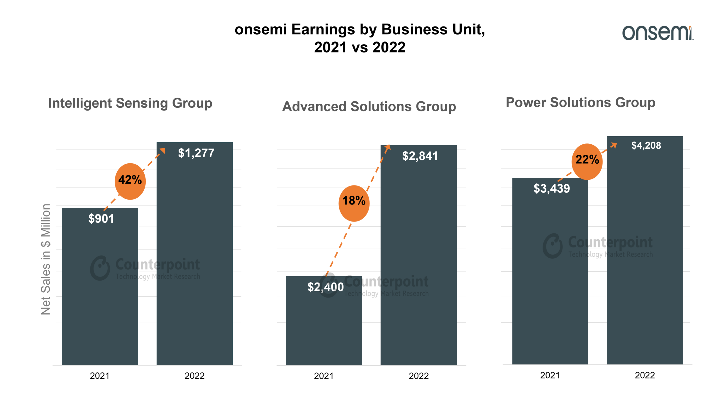
Sensing, Power Solutions Drive onsemi’s Record Revenue in 2022
2022 highlights
- Delivered a record revenue of $8.3 billion at 24% YoY growth, primarily driven by strength in automotive and industrial businesses.
- Reduction in price-to-value discrepancies, exiting volatile and competitive businesses and pivoting portfolio to high-margin products helped onsemi deliver strong earnings.
- Revenue from auto and industrial end-markets increased 38% YoY to $ 4 billion and accounted for 68% of total revenues.
- Intelligent Sensing Group revenue increased 42% YoY to $1.28 billion driven by the transition to higher-resolution sensors at elevated ASPs.
- Non-GAAP gross margin was at 49.2%, an increase of 880 basis points YoY. The expansion was driven by manufacturing efficiencies, favorable mix and pricing, and reallocation of capacity to strategic and high-margin products.
- Revenue from silicon carbide (SiC) shipments in 2022 was more than $200 million.
- Revenue committed from SiC solutions through LTSAs increased to $4.5 billion.
- Total LTSAs across the entire portfolio were at $16.6 billion exiting 2022.
- Revenue from new product sales increased by 34% YoY.
- Design wins increased 38% YoY.
Subscribe to:
Posts (Atom)