Friday, April 28, 2023

Another article on Panasonic's organic image sensor

PetaPixel: https://petapixel.com/2023/04/11/panasonics-decade-old-organic-cmos-sensor-is-still-years-away/

Panasonic’s Decade-Old Organic CMOS Sensor is Still Years Away

As a quick reminder, Panasonic's patented technology relies on an organic thin-film photo-conversion material in lieu of the conventional technique where a silicon photodiode converts light into electrical charge.

Some excerpts from the article are below.


... it has been nearly 10 years since the company first announced it was working on this new sensor and in that time, a lot has changed. The previously exciting low light capabilities have since been realized by other sensors...


[In an updated announcement last year Panasonic suggested ...] 8K resolution while retaining those dynamic range promises and would do so at high framerates. More recently, Panasonic explained that the sensor would also feature what is known as “reduced crosstalk,” which basically means that the red, green, and blue pixels of the sensor collect only their intended color and that light, regardless of type and color cast, and won’t spill across each pixel. This results in better color reproduction.
...

Basically, it’s very difficult to get excited about Panasonic’s organic CMOS, and that would be the case even if it was coming to market this year.
...

There are those who have been saying Sigma’s Foveon sensor is stuck in “development hell,” but Panasonic easily has it beat with its organic CMOS. 

Wednesday, April 26, 2023

NEC develops carbon nanotubes-based IR sensor

From StatNano: https://statnano.com/news/72257/NEC-Develops-the-World's-First-Highly-Sensitive-Uncooled-Infrared-Image-Sensor-Utilizing-Carbon-Nanotubes


NEC Develops the World's First Highly Sensitive Uncooled Infrared Image Sensor Utilizing Carbon Nanotubes

NEC Corporation has succeeded in developing the world's first high-sensitivity uncooled infrared image sensor that uses high-purity semiconducting carbon nanotubes (CNTs) in the infrared detection area. This was accomplished using NEC’s proprietary extraction technology. NEC will work toward the practical application of this image sensor in 2025.


Infrared image sensors convert infrared rays into electrical signals to acquire necessary information, and can detect infrared rays emitted from people and objects even in the dark. Therefore, infrared image sensors are utilized in various fields to provide a safe and secure social infrastructure, such as night vision to support automobiles driving in the darkness, aircraft navigation support systems and security cameras.

There are two types of infrared image sensors, the "cooled type," which operates at extremely low temperatures, and the "uncooled type," which operates near room temperature. The cooled type is highly sensitive and responsive, but requires a cooler, which is large, expensive, consumes a great deal of electricity, and requires regular maintenance. On the other hand, the uncooled type does not require a cooler, enabling it to be compact, inexpensive, and to consume low power, but it has the issues of inferior sensitivity and resolution compared to the cooled type.

(Left) Electron micrograph and image of single-walled CNTs, (Right) Atomic microscope image of a high-purity semiconducting CNT film.


(Left) Device structure, (Right) Photograph of CNT infrared array device.

In 1991, NEC discovered CNTs for the first time in the world and is now a leader in research and development related to nanotechnology. In 2018, NEC developed a proprietary technology to extract only semiconducting-type CNTs at high purity from single-walled CNTs that have a mixture of metallic and semiconducting types. NEC then discovered that thin films of semiconducting-type CNTs extracted with this technology have a large temperature coefficient of resistance (TCR) near room temperature.
The newly developed infrared image sensor is the result of these achievements and know-how. NEC applied semiconductor-type CNTs based on its proprietary technology that features a high TCR, which is an important index for high sensitivity. As a result, the new sensor achieves more than three times higher sensitivity than mainstream uncooled infrared image sensors using vanadium oxide or amorphous silicon.

The new device structure was achieved by combining the thermal separation structure used in uncooled infrared image sensors, the Micro Electro Mechanical Systems (MEMS) device technology used to realize this structure, and the CNT printing and manufacturing technology cultivated over many years for printed transistors, etc. As a result, NEC has succeeded in operating a high-definition uncooled infrared image sensor of 640 x 480 pixels by arraying the components of the structure.

Part of this work was done in collaboration with Japan’s National Institute of Advanced Industrial Science and Technology (AIST). In addition, a part of this achievement was supported by JPJ004596, a security technology research promotion program conducted by Japan’s Acquisition, Technology & Logistics Agency (ATLA).

Going forward, NEC will continue its research and development to further advance infrared image sensor technologies and to realize products and services that can contribute to various fields and areas of society.

Monday, April 24, 2023

Sony AITRIOS wins award at tinyML 2023

Link: https://www.aitrios.sony-semicon.com/en/news/aitrios-to-win-tinyml-awards-2023/ 

At the tinyML Summit 2023, held from March 27 to 29, 2023, Sony Semiconductor Solutions' edge AI sensing platform service, AITRIOS™, won the tinyML Awards 2023 "Best Innovative Software Enablement and Tools".

The tinyML Summit is a global conference on tiny machine learning (TinyML), held since 2019, where business leaders, engineers, and researchers gather to share information on the latest TinyML technologies and applications. This year the conference was held in San Francisco, United States. This award is presented to an individual, team, or organization that has created innovative software tools or development support tools related to TinyML and has contributed to the evolution of this technology.


 Deploying Visual AI Solutions in the Retail Industry
Mark HANSON , VP of Technology and Business Innovation, Sony Semiconductor Solutions of America
An image sensor with AI-processing capability is a novel architecture that is pushing vision AI closer to the edge to enable applications at scale. Today many AI applications stall in the PoC stage and never reach commercial deployment to solve real-world problems because existing systems lack simplicity, flexibility, affordability, and commercial-grade reliability. We’ll investigate why the retail industry struggles to keep track of stock on its retail shelves while relying on retail employees to manually monitor stock and how our (AITRIOS) vision AI application for on-shelf-availability can eliminate complexity and inefficiency at scale.

About AITRIOS:

The name “AITRIOS” consists of the platform keyword “AI” and “Trio S,” meaning, “three S’s.” Through AITRIOS, SSS aims to deliver the three S’s of “Solution,” “Social Value,” and “Sustainability” to the world.

Through this platform, SSS seeks to facilitate development of optimal systems, in which the edge and the cloud function in synergy, to support its partners in popularizing and expanding environmentally conscious sensing solutions using edge AI, and to deliver new value and help solve challenges faced by various industries.


AITRIOS integrates an AI model and application development environment, a marketplace, cloud-based services , and other items required for solution development into a powerful and flexible platform.

SSS, a leading company in image sensors, offers sensor configurations optimized for edge AI, enabling partners to build high-performance and reliable solutions.

AITRIOS is a one-stop B2B* (business to business) platform providing tools and environments that facilitate software and application development and system implementation.

*This service is not currently available to individual customers.

Friday, April 21, 2023

Canon's 3.2 MP SPAD Camera: Specifications

Canon's 3.2 MP SPAD camera has received some press coverage:

PetaPixel: https://petapixel.com/2023/04/03/canons-new-sensor-enables-long-range-night-vision-capabilities/

YMCinema: https://ymcinema.com/2023/04/03/canon-develops-interchangeable-lens-camera-that-sees-in-the-dark/ 

Unfortunately I have not been able to find a spec sheet. The next best thing for now is to see the 2021 IEDM proceedings paper titled "3.2 Megapixel 3D-Stacked Charge Focusing SPAD for Low-Light Imaging and Depth Sensing" (Morimoto et al., Canon Inc., Japan).  Thanks to Prof. Eric Fossum for pointing this out in a comment on an earlier post!

Abstract:
We present a new generation of scalable photon counting image sensors, featuring zero read noise and 100ps temporal resolution. Newly proposed charge focusing single-photon avalanche diode (SPAD) is employed to resolve critical trade-offs in conventional SPAD pixels. A prototype 3.2 megapixel 3D-stacked backside-illuminated (BSI) image sensor with 1-inch format demonstrates the best-in-class photon detection efficiency (PDE), dark count rate (DCR) and timing jitter performance with the largest array size ever reported in avalanche photodiode (APD)-based image sensors. The proposed technology paves the way to compact and high-definition photon counting image sensors for low-light imaging and 3D time-of-flight sensing.


Wednesday, April 19, 2023

"ai-CMOS" 9-channel color camera

From Transformative Optics Corporation: https://www.ai-cmos.com/

ai-CMOS sensors solve many of today’s challenges with antiquated CMOS technology, offering unprecedented accuracy, an expanded spectrum, plus 9-channel AI-optimized color. Extending beyond the visible spectrum into near-ultraviolet (NUV) and near-infrared (NIR) greatly expands capabilities for mobile photography, autonomous transport, and machine vision.

With higher sensitivity than Bayer sensors, near-complete color gamut, and expansion beyond visible light to near-infrared and ultraviolet frequencies, ai-CMOS brings a unique multispectral ability to standard cameras.


Mobile Photography.
Close the gap between performance and portability, while unlocking new potential for AI-powered apps.
More Contrast: Improved Black and White Modulation Transfer Function (MTF)
Broader Spectrum: Extension to Near Infrared (NIR) and Near Ultraviolet channel
Near-Complete Color Gamut: Improving color accuracy, automated white balance
Enhanced Sensitivity: Twice the Light. Lower light levels, less motion blur, plus twice the signal levels for a myriad of Integrated Signal Processing functions.

Machine Vision.
ai-CMOS offers AI applications richer and more complete data sets for training, object detection, and object classification.
Richer Data: 3x the information over Bayer
AI Optimizations: increased raw data content for feature vectors and 2x the signal strength for Integrated Signal Processing aiding apps like Super-Resolution
More Contrast: Improved Black and White Modulation Transfer Function (MTF)
Broader Spectrum: Extension to Near Infrared (NIR) and Near Ultraviolet channels

Automotive.
ai-CMOS captures more detailed data in low-light conditions, at night, and in poorer weather conditions, like fog and rain.
Spectral Sensitivity: ai-CMOS captures twice the light of current ADAS CMOS technology on the market.
Object Detection: 25% color gamut increase and 3x Feature Vectors from traditional sensors, greatly enhancing object detection and classification.
Autonomous Driving: Better enable autonomous vehicles to navigate more complex environments, and interact with other vehicles and pedestrians.


Sensor Specs.

Resolution: 3000 x 3864
Pixel Size: 8um
Sensor Format: 35mm (dia. 39.3mm)
Spectral Response: 350nm to 850nm
Quantum Efficiency: >90%
Illumination-type: BSI
Frame Rate: 30fps in HDR
Full Well: >65,000 e-
Gain Mode: HDR and Dual Gain
 

Available in limited quantities in 2023.

Monday, April 17, 2023

SWIR imaging market 'worth $2.9BN by 2028'

From optics.org news: https://optics.org/news/14/4/15

12 Apr 2023
Yole Intelligence says that the war in Ukraine and tensions over Taiwan will push defense applications beyond prior expectations.

Analysts at France-based Yole Intelligence say the current niche market for short-wave infrared (SWIR) imaging technology will grow rapidly over the next five years, and will be worth $2.9 billion by 2028.

In a new report on the segment, which is currently dominated by applications in defense, research, and industry, Yole’s Alex Clouet suggests that SWIR technology could begin replacing near-infrared (NIR) imagers in high-end smart phones, where the technology is used for secure identification.
Together with higher growth than previously expected in the military arena, plus innovation in key component materials expected to reduce costs, the upshot is expected to be a compound annual growth rate in excess of 40 per cent over the next few years.


Although definitions of SWIR and NIR spectral ranges differ, the term SWIR is often used to refer to wavelengths between 1400 nm and 3000 nm, whereas NIR relates to the 780-1400 nm band.
According to the report, the SWIR imaging market was worth just over $300 million last year, with defense, aerospace, and research applications accounting for more than two-thirds of that total.
“The defense segment will experience higher growth than previously expected, reaching $405 million in 2028 from $228 million in 2022, pulled by geopolitical tensions such as the Ukraine war and tensions around Taiwan and an increasing number of countries becoming interested in SWIR technologies,” Yole says.

The current focus means that defense-oriented players such as Israel’s SCD, Sensors Unlimited, and Teledyne FLIR dominate the scene. But as the technology begins to find use in a larger number of industrial and consumer applications, that is likely to change.

“Many smaller players have significant growth potential, like Sony, or companies making quantum-dot-based cameras, such as SWIR Vision Systems and Emberion, which have a price advantage on high-resolution and extended spectral range products,” Yole stated.

“Newcomers bring new disruptive technologies, like STMicroelectronics, TriEye, or Artilux, to address consumer or automotive markets.”

Emberion, which is a spin-out from Nokia with facilities in Cambridge, UK, uses both colloidal quantum dots and graphene in its devices - claiming improvements in signal-to-noise, breadth of spectral response, and operating temperature.

“Traditional CMOS image sensor suppliers can be game-changers due to their high-volume production capacity and unique design and integration know-how,” observes Yole.
“However, among them, only Sony and STMicroelectronics have already developed SWIR imaging technology - even though others may show signs of interest, such as Samsung and OmniVision.
“The SWIR ecosystem waits for greater interest from these players to accelerate technological and market disruption.”


Material innovation
Nevertheless, the technology is expected to make an impact in consumer goods, with Yole’s figures suggesting the emergence of a significant consumer market over the next five years.
“In 2026, SWIR can start replacing NIR imagers in flagship smart phones for under-display integration of facial recognition modules,” reckons Clouet, adding that the resulting market for complete 3D-sensing modules will just surpass $2 billion by 2028.
Beyond that - and depending on the level of innovation and cost reductions in key components - the technology might end up being integrated into lower-end smart phones and augmented and virtual reality (AR/VR) headsets to improve the performance of tracking cameras, 3D sensing, and outdoor multispectral imaging.

Clouet also sees applications emerging in the automotive sector, where SWIR could provide enhanced vision in low light and adverse weather conditions, as well as 3D sensing capability - although this market would still be in its infancy by 2028.

Among the technological innovations that may lead to more efficient and lower-cost imaging systems, Yole highlights the potential of quantum dots, organic photodiodes, and the germanium-on-silicon material system as some potentially key developments in sensors.
At the optical component level, polymer and metasurface lenses, diffractive optics and optical diffusers, and spectral filters could also contribute to lower costs.

Yole's report, SWIR Imaging 2023, is available now via the company’s web site.


Friday, April 14, 2023

SWIR linear array sensor from NIT

Press release from NIT:


The NSC1801 line scan sensor was designed initially for imaging linearly moving objects with high frame rate, high sensitivity and low noise. Its pixel size has the world smallest size of 7.5µm that contributes the lower the manufacturing costs without increasing the cost of lenses.

Now NIT is pleased to release an updated version of NSC1801, where all key parameters have been reworked and overall performances improved. NSC1801 is currently installed in NIT Lisa SWIR cameras.

NSC1801 fully benefits from NIT new manufacturing factory installed in our brand new clean room, that includes our high yield hybridization process. Our new facility allows to cover the full design and manufacturing cycle of these sensors in volume with a level of quality never achieved before. 

Moreover NSC1801 was designed with the objective of addressing new markets that could not invest into expensive and difficult to use SWIR cameras. The result is that our Lisa SWIR camera based on NSC1801 exhibits the lowest price point on the market even in unit quantity.  

Typical applications for NSC1801 are waste sorting, semiconductor and photovoltaic cell inspection, food and vegetable inspection and pharmaceutical inspection. 


Features

Benefits

Pixel size 7.5x7.5µm

Lowest pixel size in the industry to capture sharp details

Resolution 2048 pixels

Large field of view compatible with most lenses from the market

Three gain modes available

Allows selecting the best dynamic range for the scene. 

QE >85%

Boost sensitivity to the maximum available

Line rate up to 60KHz

For imaging fast moving objects 

Exposure time 10µs to 220ms

Fully configurable for capturing the best signal to noise ratio


Wednesday, April 12, 2023

Canon to start selling 3.2MP SPAD sensor in 2023

Canon developing world-first ultra-high-sensitivity ILC equipped with SPAD sensor, supporting precise monitoring through clear color image capture of subjects several km away, even in darkness

TOKYO, April 3, 2023—Canon Inc. announced today that the company is developing the MS-500, the world's first1 ultra-high-sensitivity interchangeable-lens camera (ILC) equipped with a 1.0 inch Single Photon Avalanche Diode (SPAD) sensor2 featuring the world's highest pixel count of 3.2 megapixels3. The camera leverages the special characteristics of SPAD sensors to achieve superb low-light performance while also utilizing broadcast lenses that feature high performance at telephoto-range focal lengths. Thanks to such advantages, the MS-500 is expected to be ideal for such applications as high-precision monitoring.

There is a growing need for high-precision monitoring systems for use in such environments as national borders, seaports, airports, train stations, power plants and other key infrastructure facilities, in order to quickly identify targets even under adverse conditions including darkness in which human eyes cannot see, and from long distances.

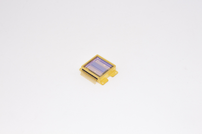
The currently in-development MS-500 is equipped with a 1.0 inch SPAD sensor that reduces noise, thus making possible clear, full-color HD imaging even in extreme low-light environments. When paired with Canon's extensive range of broadcast lenses, which excel at super-telephoto image capture, the camera is capable of accurately capturing subjects with precision in extreme low-light environments, even from great distances. For example, the camera may be used for nighttime monitoring of seaports, thanks to its ability to spot vessels that are several km away, thus enabling identification and high-precision monitoring of vessels in or around the seaport.

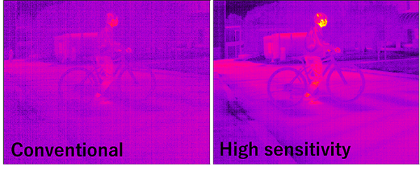
With CMOS sensors, which are commonly used in conventional modern digital cameras, each pixel measures the amount of light that reaches the pixel within a given time. However, the readout of the accumulated electronic charge contains electronic noise, which diminishes image quality, due to the process by which accumulated light is measured. This leads to degradation of the resulting image, particularly when used in low-light environments. SPAD sensors, meanwhile, employ a technology known as "photon counting", in which light particles (photons) that enter each individual pixel are counted. When even a single photon enters a pixel, it is instantly amplified approximately 1 million times and output as an electrical signal. Every single one of these photons can be digitally counted, thus making possible zero-noise during signal readout—a key advantage of SPAD sensors4. Because of this technological advantage, the MS-500 is able to operate even under nighttime environments with no ambient starlight5, and is also capable of accurately detecting subjects with minimal illumination and capture clear color images.


The MS-500 employs the bayonet lens mount (based on BTA S-1005B standards) which is widely used in the broadcast lens industry. This enables the camera to be used with Canon's extensive range of broadcast lenses which feature superb optical performance. As a result, the camera is able to recognize and capture subjects that are several km away.

Going forward, Canon will continue to pursue R&D and create products capable of surpassing the limits of the human eye while contributing to the safety and security of society by leveraging its long history of comprehensive imaging technologies that include optics, sensors, image processing and image analysis.

Canon plans to commence sales of the MS-500 in 2023.

Reference

The MS-500 will be displayed as a reference exhibit at the Canon booth during the 2023 NAB Show for broadcast and filmmaking equipment, to be held in Las Vegas from Saturday, April 15 to Wednesday, April 19.

 1Among color cameras. As of April 2, 2023. Based on Canon research.

 2Among SPAD sensors for imaging use. As of April 2, 2023. Based on Canon research.

 3Total pixel count: 3.2 million pixels. Effective pixel count: 2.1 million pixels.

 4For more information on how SPAD sensors operate and how they differ from CMOS sensors, please visit the following website:

 https://global.canon/en/technology/spad-sensor-2021.html

 5Ambient starlight is equivalent to approximately 0.02 lux. A nighttime environment with no ambient starlight is equivalent to approximately 0.007 lux.

Monday, April 10, 2023

Metalenz polarization sensor wins SPIE award

https://metalenz.com/metalenz-wins-2023-prism-award/

San Francisco, CA – SPIE, the international society for optics and photonics, recognized the most innovative new optics and photonics products with the annual industry-focused Prism Awards. Metalenz was named winner of the Camera and Imaging category for PolarEyes, the Company’s breakthough polarization imaging platform designed around the unique capabilities of Metalenz meta-optics.

PolarEyes is the world’s first and only optical module that can instantly provide information about the material make-up and depth details of the imaged scene, thereby providing highly valuable, previously unavailable information to machine vision systems.

Traditional approaches to polarization imaging require a complex array of optics, waveplates and filters, resulting in modules that are too large, expensive, and inefficient for mass markets or small form-factor devices. Dr. Noah Rubin and Professor Federico Capasso demonstrated in foundational research that a single meta-optic can complete image all of the polarization information in a scene without filtering or loss of efficiency. Now, the team at Metalenz has productized this breakthrough with PolarEyes. The result is a full-Stokes polarization camera that is over 5000x more compact than traditional cameras. This brings powerful lab camera capabilities into tiny camera modules that fit into any smart or mobile device. More than a polarized meta-optic, this full-stack, system-level solution combines physics and optics, software and hardware to power machine vision systems for next-generation smartphones and consumer electronics, to new automotive, robotic and healthcare applications.

“We are honored to have this recognition from SPIE and the photonics community. With PolarEyes, we are using our metasurface technology to look beyond just solving size and performance in existing sensor modules. We are empowering billions of devices with new information that will change the way that people and machines interact with and understand the world.” Rob Devlin, Metalenz Co-founder and CEO.


More information from: https://metalenz.com/polareyes-polarization-imaging-system/

Metalenz's "PolarEyes" polarization-based imaging system is a microscopic sensing solution that harnesses the power of polarized light. PolarEyes characterizes depth, material properties and detects transparent objects–bringing new information to a mobile form factor for the first time.

Traditional approaches to polarization imaging require a complex array of light splitters and filters, resulting in modules that are too large, expensive and inefficient for mass markets or small form-factor devices. PolarEyes shrinks these powerful lab cameras into tiny camera modules that fit into any smart or mobile device.


PolarEyes captures polarized light without filtering or loss of signal strength, and the full-stack, system-level solution combines physics and optics, software and hardware to power machine vision systems for next-generation smartphones and consumer electronics, to new automotive, robotic and healthcare applications.


Polarization provides an additional scene cue beyond intensity and depth which can be used for material classification, improved 3D sensing (surface normal reconstruction) and removing glare. Use cases include consumer electronics, robotics and automotive.

Friday, April 07, 2023

EETimes article on LiDAR for ADAS

EETimes article argues that LiDARs will be an important component in future ADAS systems.

Link: https://www.eetimes.com/the-future-of-lidar-lies-in-adas/ 

Cars are becoming more and more autonomous, to the point that self-driving is getting close to becoming real. High-performance sensors have enabled an ever-increasing number of advanced driver-assistance system (ADAS) features, such as lane-keeping, adaptive cruise control and structures for detecting blind spots during overtaking.

ADAS serves as a useful tool for drivers as well as a response to the demand for improved safety requirements. LiDAR is one of the most important components of ADAS, as it can be used in adaptive cruise control, blind-spot detection, pedestrian detection and all use cases that require the detection and mapping of objects around the vehicle.

ADAS, which corresponds to Level 2 of the driving automation scale, is now standard in most cars. Sensors that can deliver a high level of safety are required for autonomous or semi-autonomous vehicles. For automotive applications, this means that the sensor must be reliable in all-weather situations and unaffected by factors like sun, rain or fog. LiDAR sensors are also appropriate for use in high-vibration transport systems, such as driverless vehicles, mining, building and agriculture.

The article goes on to discuss two recent trends: solid-state LiDARs and spectrum-scan LiDARs.

Recently, we have witnessed a growing interest in solid-state LiDAR technology, i.e., a system that uses a laser source and a detector and that does not include scanning nor moving parts. Solid-state technology gradually measures and acquires the surrounding environment instead of depending on sequential measurements to send laser light in one direction, gather measurements and then change to another place, as in conventional optical LiDAR.

...

The Spectrum-Scan proprietary platform created by Baraja takes a distinct approach from traditional mechanical LiDAR systems. Instead of employing flimsy moving parts and oscillating mirrors to scan the surrounding area, refraction of light through prism-like optics is used. On the other hand, mechanically scanned sensors in the fast axis have expensive, large and prone-to-failure moving parts.

Wednesday, April 05, 2023

XenomatiX solid-state LiDAR

Link: https://xenomatix.com/lidar/xenolidar/


XenomatiX, pioneer of true-solid-state LiDARs for ADAS, AVs and road applications launched the new generation true-solid-state XenoLidar-X for automotive and industrial applications. XenoLidar-X is small, fast, light, and delivers high resolution with low power consumption. These characteristics make it suitable for integration and series applications.

The webpage discloses the following specs:

Range: up to 50 m
Field of view: 60°x20°
Angular resolution: 0.3° x 0.3°
Data output rate: 20 Hz

Monday, April 03, 2023

Quantum Dot-based image sensors (IEEE TED June 2022 issue)

Two papers in the IEEE Trans. Electron Devices journal from June 2022 on the topic of infrared quantum dot-based image sensors.

Infrared Colloidal Quantum Dot Image Sensors
Pejović et al. (IMEC Belgium)


Quantum dots (QDs) have been explored for many photonic applications, both as emitters and absorbers. Thanks to the bandgap tunability and ease of processing, they are prominent candidates to disrupt the field of imaging. This review article illustrates the state of technology for infrared image sensors based on colloidal QD absorbers. Up to now, this wavelength range has been dominated by III–V and II–VI imagers realized using flip-chip bonding. Monolithic integration of QDs with the readout chip promises to make short-wave infrared (SWIR) imaging accessible to applications that could previously not even consider this modality. Furthermore, QD sensors show already state-of-the-art figures of merit, such as sub-2- μm pixel pitch and multimegapixel resolution. External quantum efficiencies already exceed 60% at 1400 nm. With the potential to increase the spectrum into extended SWIR and even mid-wave infrared, QD imagers are a very interesting and dynamic technology segment.

Different layers in a QD image sensor


Representative images made by different QD image sensors. (a) PbS QD, SWIR image (cutoff at 1.6 μm ), 5-μm pixel pitch, and data courtesy of IMEC. (b) PbS QD, SWIR image (cutoff at 2 μm ), 15-μm pixel pitch, and data courtesy of SWIR vision systems. (c) PbS QD, SWIR image (cutoff at 2 μm ), 20-μm pixel pitch, and data courtesy of Emberion. (d) PbS QD, SWIR image (cutoff at 1.6 μm ), 2.2-μm pixel pitch, and data courtesy of STMicroelectronics. (e) PbS QD, SWIR image (cutoff at 1.85 μm ), and data courtesy of ICFO. (f) HgTe QD, MWIR image (cutoff at 5 μm ), 30-μm pixel pitch, and reprinted with permission from [51]. (g) HgTe QD, SWIR image (cutoff at 2 μm ), half VGA, 15-μm pixel pitch, and data courtesy of Sorbonne University.


Figures of Merit of Five Different PbS QD Image Sensors


Detailed Characterization of Short-Wave Infrared Colloidal Quantum Dot Image Sensors
Kim et al. (IMEC, Belgium)


Thin-film-based image sensors feature a thin-film photodiode (PD) monolithically integrated on CMOS readout circuitry. They are getting significant attention as an imaging platform for wavelengths beyond the reach of Si PDs, i.e., for photon energies lower than 1.12 eV. Among the promising candidates for converting low-energy photons to electric charge carriers, lead sulfide (PbS) colloidal quantum dot (CQD) photodetectors are particularly well suited. However, despite the dynamic research activities in the development of these thin-film-based image sensors, no in-depth study has been published on their imaging characteristics. In this work, we present an elaborate analysis of the performance of our short-wave infrared (SWIR) sensitive PbS CQD imagers, which achieve external quantum efficiency (EQE) up to 40% at the wavelength of 1450 nm. Image lag is characterized and compared with the temporal photoresponsivity of the PD. We show that blooming is suppressed because of the restricted pixel-to-pixel movement of the photo-generated charge carriers within the bottom transport layer (BTL) of the PD stack. Finally, we perform statistical analysis of the activation energy for CQD by dark current spectroscopy (DCS), which is an implementation of a well-known methodology in Si-based imagers for defect engineering to a new class of imagers.

(a) QDPD stack integration on the Si-ROIC. (b) Structure schematic of its passive PD-only device without the ROIC (ECL: edge cover layer, figures not scaled).


(a) Typical PTC for our PbS QDPD imager displaying a shot-noise-limited behavior in the relatively intense light illumination condition. (b) EQE measured with a PD-only passive device (red dashed), with an imager (black), showing no significant change in their spectral shapes and values.


Image of the Imec campus taken with our QDPD imager on a visibly sunny day with the collection of photons in the visible spectral range [(a) < 750 nm], and in the SWIR wavelengths [(b) >1350 nm], showing bright and dark sky respectively since photons with lower energy (SWIR) are less scattered by air molecules and do not reach to the imager. Set of images capturing objects under the illumination of visible [(c) < 750 nm] and SWIR [(d) >1350 nm] light. While two plastic bars are less distinguished under visible light, they have clear contrast in the SWIR range, since the Bar #2 is more optically reflective compared with Bar #1 in that spectral region.


(a) Arrhenius plot from the PbS CQD imager pixel data (Gen 1 stack). Approximately 0.41 eV of activation energy is fitted from this plot made of median dark outputs of individual pixels. (b) Activation energy histogram computed from individual pixels, showing multiple peaks ranging from 0.23 to 0.43 eV. (c) Dark current propagation according to the temperature elevation for 0°C (left), 40°C (middle), and 80°C (right), respectively.