Autosens publishes a number of the interviews from its conference held in Detroin in May this year:
Friday, May 31, 2019
Video from Lensless Stills
Arxiv.org paper "Video from Stills: Lensless Imaging with Rolling Shutter" by Nick Antipa, Patrick Oare, Emrah Bostan, Ren Ng, and Laura Waller from UCB pulls a high speed 4,500fps video from a rolling shutter stills sensor:
"Because image sensor chips have a finite bandwidth with which to read out pixels, recording video typically requires a trade-off between frame rate and pixel count. Compressed sensing techniques can circumvent this trade-off by assuming that the image is compressible. Here, we propose using multiplexing optics to spatially compress the scene, enabling information about the whole scene to be sampled from a row of sensor pixels, which can be read off quickly via a rolling shutter CMOS sensor. Conveniently, such multiplexing can be achieved with a simple lensless, diffuser-based imaging system. Using sparse recovery methods, we are able to recover 140 video frames at over 4,500 frames per second, all from a single captured image with a rolling shutter sensor. Our proof-of-concept system uses easily-fabricated diffusers paired with an off-the-shelf sensor. The resulting prototype enables compressive encoding of high frame rate video into a single rolling shutter exposure, and exceeds the sampling-limited performance of an equivalent global shutter system for sufficiently sparse objects."


"Because image sensor chips have a finite bandwidth with which to read out pixels, recording video typically requires a trade-off between frame rate and pixel count. Compressed sensing techniques can circumvent this trade-off by assuming that the image is compressible. Here, we propose using multiplexing optics to spatially compress the scene, enabling information about the whole scene to be sampled from a row of sensor pixels, which can be read off quickly via a rolling shutter CMOS sensor. Conveniently, such multiplexing can be achieved with a simple lensless, diffuser-based imaging system. Using sparse recovery methods, we are able to recover 140 video frames at over 4,500 frames per second, all from a single captured image with a rolling shutter sensor. Our proof-of-concept system uses easily-fabricated diffusers paired with an off-the-shelf sensor. The resulting prototype enables compressive encoding of high frame rate video into a single rolling shutter exposure, and exceeds the sampling-limited performance of an equivalent global shutter system for sufficiently sparse objects."


Daiwa: The More the Merrier: Multi-Cameras Trend in Smartphones
Taiwan branch of Daiwa Capital Markets publishes report "The more the merrier: multi-cameras are the next mega trend in smartphones" dated by Oct. 2018. Few charts and tables form the report:


Triple Cameras Technology challenges, according to Daiwa:


Triple Cameras Technology challenges, according to Daiwa:
- Calibration. The cameras need to be carefully calibrated for optical properties of a triple aperture system. The calibration consists of recovering camera parameters, location and orientation for external parameters and focal lengths for internal parameters. In addition, the calibration should be completed in the camera manufacturing line for numerous tests on any dynamic physical changes, such as temperature variances and drop test.
- Firmware/algorithm. A triple-cam system demands more complexity on the firmware side as the framework in a triple-cam system will have to deal with each of the 3 cameras to operate as one integrated camera. In addition, algorithms would have the same challenges to ensure reasonable processing run time and also maintain zero distortion of the image quality from multiple inputs.
- Power consumption. The complex algorithm and firmware, which require more processing power in power management, frame request and memory management, could lead to higher power consumption for the entire camera system (camera + processing platform).
Thursday, May 30, 2019
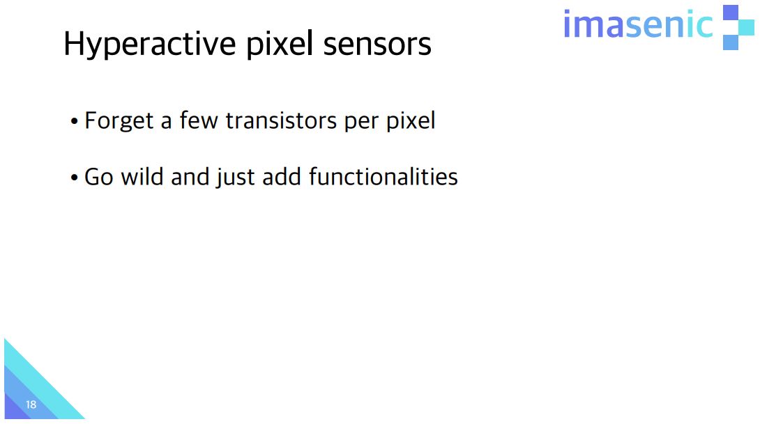
Imasenic on Smart Image Sensors
Renato Turchetta, CEO of Imasenic, presented "Smart CMOS Image Sensors" at Workshop on the Architecture of Smart Cameras, held on 27-28 June 2018, Coimbra, Portugal. Below are just few slides from the 57-page presentation:


Wednesday, May 29, 2019
Greenthread Sues Samsung over Patents Infringement
Greenthread LLC files patent infringement lawsuit against Samsung:
"The Greenthread Patents cover foundational semiconductor technologies in the design and manufacture of integrated circuits such as memory, including but not limited to DRAM and NAND flash, and image sensors. Specifically, the Greenthread Patents describe semiconductor devices that employ graded dopants and well regions for, e.g., creating electric fields for aiding and/or retarding the movement of carriers to and/or from the semiconductor surface to/from the semiconductor substrate."
Few patents mentioned in the filing list G. R. Mohan Rao as an inventor:
US8421195B2 “Semiconductor Devices with Graded Dopant Regions”
US8106481B2 “Semiconductor Devices with Graded Dopant Regions”
US9647070B2 “Semiconductor Devices with Graded Dopant Regions”
The filing has an interesting info about Samsung S5K2X7SP sensor that allegedly infringes on the '070 patent above. This is fairly modern 24MP 0.9um Tetracell sensor featuring DTI, vertical transfer gate (VTG), and many other recent innovations from Samsung:
"Upon information and belief, the Accused Image Sensor Instrumentalities are in relevant part substantially similar to the exemplary S5K2X7SP CMOS image sensor, in particular with regard to the manner in which the Accused Image Sensor Instrumentalities include and utilize regions with graded dopant concentrations. Upon information and belief, Samsung fabricates the Accused Image Sensor Instrumentalities according to processes that utilize substantially similar process steps, including process steps for creating regions with graded dopant concentrations."
Automotive SWIR Startup Trieye Raises $17M
VentureBeat, Reuters, Globes, TechTime: Israel-based SWIR image sensor startup TriEye announces a $17M financing round led by Intel Capital. The new funds will be used to develop its sensors for low-visibility situations for connected and autonomous vehicles.
TriEye's SWIR technology is CMOS-based, enabling the scalable mass-production of SWIR sensors and reducing the cost by a factor of 1,000x compared to InGaAs-based technology. The initial SWIR camera samples are expected to enter the market in 2020.


TriEye's SWIR technology is CMOS-based, enabling the scalable mass-production of SWIR sensors and reducing the cost by a factor of 1,000x compared to InGaAs-based technology. The initial SWIR camera samples are expected to enter the market in 2020.


Tuesday, May 28, 2019


Celepixel Demos
Celepixel demos its event-based sensors in different conditions:
More video examples can be found in the company's 2016 video.
More video examples can be found in the company's 2016 video.
Monday, May 27, 2019
3D Imaging News: Ams, Infineon, Etron
IEEE Spectrum publishes Ams article "3 Types of 3D Sensing for Smartphones and Self-Driving Cars" by Markus Rossi, VP for innovations in optical sensors. Few quotes:
"Structured light cameras project patterns of light onto objects and analyze distortions in the reflection. Time-of-flight sensors measure the time it takes for light to travel to and from an object as a way to discern its distance. And active stereo vision combines two or more types of near-infrared cameras to triangulate the location and movements of an object.
Facial recognition is today the primary application of 3D sensing... But 3D sensing is also becoming important in the automotive sector, both outside the vehicle as well as inside.
In general, detecting reflected light (from dots or flood illumination) at close distance (say, 40 to 60 cm) is not a major challenge for current systems. And these systems are defined to work in a number of different scenarios. The most critical one is outdoors—the intensity of the reflected dots needs to be strong enough that it can be detected when the light sensor is also being flooded with sunlight.
Calibration is very important for all three technologies—both factory calibration as well as real-time calibration... For example, in order to do triangulation through stereo vision, the cameras need to be positioned at a certain base line (typically in the range of 25 mm). This distance needs to stay constant down to a micron or a fraction of a micron apart. A mechanical shock or a slight variation in temperature could affect their performance."
Infineon: The Embedded Vision Alliance awarded Infineon 3D ToF single chip solution as “Product of the Year” in the category “Sensors.”
“Congratulations to Infineon for winning Best Sensor in our 2019 Vision Product of the Year awards,” said Jeff Bier, Founder of the Embedded Vision Alliance. “Innovative sensor designs, like Infineon's 3D Image Sensor, are enabling new 3D vision experiences such as smartphone face recognition and augmented reality. Infineon has been a pioneer in creating 3D image sensors for visual AI applications. I applaud the company’s ongoing investment in innovation and quality in this rapidly changing and often confusing market. I’m proud that Infineon is a member of the Embedded Vision Alliance and delighted they have been recognized with this outstanding honor.”
“We would like to thank the Embedded Vision Alliance for having honored us with the ‘Product of the Year’ Award, which recognizes Infineon’s innovation and performance of our REAL3™ ToF-based 3D imager the category ‘Sensors’, said Philipp von Schierstaedt, VP, RF & Sensors, Infineon. “Building upon the combined expertise of Infineon and pmdtechnologies, the novel sensor delivers a new level of 3D camera capabilities in mobile device applications. Infineon’s REAL3TM ToF sensor enables a unique user’s experience in secure face-authentication, computational photography and seamless AR-applications.”

Digitimes: Etron started shipping production version of its 3D stereo processors and expects the shipments to top 50,000 units in May.

Shimonomura Lab Videos
Shimonomura Lab from Ritsumeikan University, Japan, publishes a couple of nice videos complementing the previously published papers.
Video illustrating Light-In-Flight paper:
It could be a good market for DVS sensors, if one places such sensor under each button in a keyboard:
I'm not sure how large is the demand for this sensor, but looks like a fresh idea:
Video illustrating Light-In-Flight paper:
It could be a good market for DVS sensors, if one places such sensor under each button in a keyboard:
I'm not sure how large is the demand for this sensor, but looks like a fresh idea:
Sunday, May 26, 2019
UBS Estimates Galaxy S10 Cameras Cost at 14-16% of BOM
IFNews publishes UBS cost analysis of Samsung Galaxy S10, S10+ and S10 e smartphones with cameras accounting for 14-16% of the BOM:


Samsung Galaxy S10 5G also features front and rear ToF cameras:
"S10 5G comes with total 4 cameras on the rear side. In addition to the same three cameras we have for S10+/S10 (12MP wide + 12MP telephoto + 16MP ultra-wide camera), the 5G model adds a Time-of-Flight module. For the ToF we think the sensor likely comes from Sony, and the module should also include one VCSEL laser which we believe is supplied by either Osram or ams AG. Interestingly for the rear side ToF, we think Sunny Optical could be the main supplier for the module, while SEMCO and Samsung are still doing the modules for the existing three cameras as well as for the combining of the final quad cam. We think the cost for the quad camera for S10 5G model could be c. $55, of which the ToF module alone could cost c. $10."

"On the front side, S10 5G also has dual front camera similar to that of S10+. One difference though is that it replaces the 8MP RGB depth camera with a Time-of-Flight. We think the ToF module structure is similar to that on the rear side: Sony likely supplying the ToF sensor, and one VCSEL laser likely supplied by Osram. We think Partron is the main module assembler for the ToF module, as well as for the combined dual camera module. We think the cost for the dual front camera for S10 5G model is c. $20, of which the ToF module alone could cost c. $10."

Automotive Camera Market
ResearchInChina report "China Passenger Car Camera Market Report, 2019Q1" says:
In China, front view monocular camera is the one largely demanded in passenger car market, with its installations in 2019Q1 surging by 71.7% from the same period of 2018, according to our recent report -- China Passenger Car Camera Market Report, 2019Q1.
The top three players Aptiv, Bosch and Denso commanded 21.3%, 16.9% and 13.0% of the market, respectively.

PRNewswire: The automotive camera market is anticipated to hike from USD 5.5 billion in 2018 to around USD 19 billion by 2025 when the global industry shipments will register 17% growth, according to a 2019 Global Market Insights, Inc. report.

Friday, May 24, 2019
Low-End Laptops to Keep VGA Camera Forever
PRNewswire: "Analysts predict that 20% of embedded notebook cameras will remain at VGA resolutions for the foreseeable future, due to cost considerations in the entry-level market," said Jason Chiang, product marketing manager at OmniVision. "By introducing this new OV0VA10 SoC with advanced pixel technology, OmniVision is increasing the performance and extending the viability of the VGA notebook camera market."
OmniVision OV0VA10 SoC integrates a VGA image sensor and signal processor in a single chip-scale package. The SoC's OmniPixel 3-HS allows entry level, thin-bezel notebook designers to incorporate the VGA camera with excellent low light image capture for applications such as videoconferencing. Additionally, it offers 30% lower power consumption than the leading competitor.
Additionally, its OmniPixel 3-HS enhances color performance with symmetric pixel design to eliminate color shading and optimize the signal-to-noise ratio. This SoC's integrated image sensor has a 1/10" optical format and 2.2um pixel size, enabling a 4mm camera module in the Y dimension for the latest entry level notebooks with thinner bezels. Additionally, it is manufactured using 200mm wafer process and is offered in an 8" chip-scale package with a DVP interface.

FT: 15% of Sony CIS Sales Go to Huawei
FT discusses the US ban on components sale to Huawei. As Panasonic and Toshiba halt shipping their chips to the Chinese company, a question arises about Sony image sensors. They are used in all Huawei flagship phones and are difficult to substitute.
When contacted, Sony executives declined to comment on that. Jefferies analyst Atul Goyal estimates that Sony image sensor sales to Huawei is about 15% of the company's total CIS production. Oppo and Vivo use Sony sensors too, so if Huawei loses its market share to them, it should not impact Sony much. However, if Samsung takes over Huawei's products, Sony sales might suffer.
When contacted, Sony executives declined to comment on that. Jefferies analyst Atul Goyal estimates that Sony image sensor sales to Huawei is about 15% of the company's total CIS production. Oppo and Vivo use Sony sensors too, so if Huawei loses its market share to them, it should not impact Sony much. However, if Samsung takes over Huawei's products, Sony sales might suffer.
Aurora Buys Blackmore
Techcrunch, Wired, Forbes-1, Forbes-2: Aurora, an AI self-driving startup that recently raised $530M in Round B, acquires Montana-based 10 year-old FMCW Doppler LiDAR developer Blackmore. The 70 Blackmore employees will join the 250 Aurora's engineers and technicians. So far, Blackmore has raises $21.5M in tow financing rounds.
“We're really the pioneers in FM lidar,” Blackmore founder and CEO Randy Reibel says. “The easiest analogy is AM radio versus FM radio. If you think back to the days of broadcast radio, AM radio has a lot of interference. It’s staticky. When you work with an FM lidar system, or an FM radio, you don’t have that interference. That’s a huge deal in this space, especially from a safety perspective. … As we start to pack the roads with hundreds and hundreds of lidars in close proximity, they’re going to crosstalk. With an FM lidar, you don’t have any of those interference challenges.”
That kind of consolidation will likely continue, Reibel predicted, in part because it’s challenging for LiDAR companies to “go it alone.” AV companies are particularly protective of their tech and opening the door to an outside LiDAR company takes convincing.
Aurora said it is not interested in manufacturing hardware, whether it’s cars or LiDARs. The company will work with automotive Tier 1 suppliers and other partners as it scales.


Thursday, May 23, 2019
Update on Ominivision and Superpix Acquisition by Will Semi
From Deloitte doc: "In 2018, Shanghai Will Semiconductor acquired a 85% stake in Beijing SuperPix Micro Technology and a 96% stake in Beijing OmniVision Technologies for USD2.18bn to take advantage of the high-end technics of OmniVision and cost control capabilities of SuperPix."
See here the previous reports on that.
See here the previous reports on that.
Yanta Research on 2018 CIS Market Shares
Korea-based Yanta Research publishes its view on CIS market shares with Hynix taking #4 spot on the chart:


Omnivision VGA NIR Camera Module
PRNewswire: OmniVision announces the OVM7251 VGA CameraCubeChip module built on the 3um OmniPixel 3-GS global shutter pixel. The module is available in an 850nm version for AR/VR eye tracking, and a 940nm version for machine vision and 3D sensing in mobile facial authentication.
“Until now, most camera modules for these applications have been built with rolling shutters, which have latency issues. Meanwhile, global shutter modules have previously been too large and expensive,” said Aaron Chiang, marketing director at OmniVision. “Our new OVM7251 overcomes these challenges by providing a cost effective VGA module with global shutter performance in a wafer-level, reflowable form factor.”
The OVM7251’s sleep current consumption is 5mA, and during active mode. The module is available now for sampling and volume production, along with an evaluation kit.

Fast Imaging in the Dark
Pixart and National Chiao Tung University, Taiwan publish an open access paper "Fast Imaging in the Dark by using Convolutional Network" by Mian Jhong Chiu, Guo-Zhen Wang, and Jen-Hui Chuang presented at 2019 IEEE International Symposium on Circuits and Systems (ISCAS):
"While fast imaging in low-light condition is crucial for surveillance and robot applications, it is still a formidable challenge to resolve the seemingly inevitable high noise level and low photon count issues. A variety of image enhancement methods such as de-blurring and de-noising have been proposed in the past. However, limitations can still be found in these methods under extreme low-light condition. To overcome such difficulty, a learning-based image enhancement approach is proposed in this paper. In order to support the development of learning-based methodology, we collected a new low-lighting dataset (less than 0.1 lux) of raw short-exposure (6.67 ms) images, as well as the corresponding long-exposure reference images. Based on such dataset, we develop a light-weight convolutional network structure which is involved with fewer parameters and has lower computation cost compared with a regular-size network. The presented work is expected to make possible the implementation of more advanced edge devices, and their applications."


"While fast imaging in low-light condition is crucial for surveillance and robot applications, it is still a formidable challenge to resolve the seemingly inevitable high noise level and low photon count issues. A variety of image enhancement methods such as de-blurring and de-noising have been proposed in the past. However, limitations can still be found in these methods under extreme low-light condition. To overcome such difficulty, a learning-based image enhancement approach is proposed in this paper. In order to support the development of learning-based methodology, we collected a new low-lighting dataset (less than 0.1 lux) of raw short-exposure (6.67 ms) images, as well as the corresponding long-exposure reference images. Based on such dataset, we develop a light-weight convolutional network structure which is involved with fewer parameters and has lower computation cost compared with a regular-size network. The presented work is expected to make possible the implementation of more advanced edge devices, and their applications."


Wednesday, May 22, 2019
Sony Opens Design Centers in Norway, Germany, and Switzerland
Sony posts the following message at LinkedIn: "Sony Semiconductor Solutions, the largest image sensor supplier in the world, is establishing new design centers across Europe (Norway, Germany, Switzerland).
The design centers will focus on the design and the development of image sensors targeting a plethora of markets including mobile, automotive and industrial. The European design teams will work closely with Sony Semiconductor design and manufacturing teams in Japan.
We are starting a wide recruitment campaign all over Europe with the purpose of hiring analogue and digital engineers as well as engineering managers and field application engineers."
Thanks to AB for the pointer!

Ge-on-Si SPAD Publications
As noted in comments to my previous post on Heriot Watt University Ge-on-Si SPADs, there is a similar work in Eduardo Charbon group in EPFL and Delft University. The most recent development is presented in open-access IEEE TED paper "CMOS-Compatible PureGaB Ge-on-Si APD Pixel Arrays" by Amir Sammak, Mahdi Aminian, Lis K. Nanver, and Edoardo Charbon:
"Pure gallium and pure boron (PureGaB) Ge-on-Si photodiodes were fabricated in a CMOS compatible process and operated in linear and avalanche mode. Three different pixel geometries with very different area-to-perimeter ratios were investigated in linear arrays of 300 pixels with each a size of 26 x 26 mu m(2). The processing of anode contacts at the anode perimeters leaving oxide covered PureGaB-only light-entrance windows, created perimeter defects that increased the vertical Ge volume but did not deteriorate the diode ideality. The dark current at 1 V reverse bias was below 35 mu A/cm(2) at room temperature and below the measurement limit of 2.5 x 10(-2) mu A/cm(2) at 77 K. Spread in dark current levels and optical gain, that reached the range of 10(6) at 77 K, was lowest for the devices with largest perimeter. All device types were reliably operational in a wide temperature range from 77 K to room temperature. The spectral sensitivity of the detectors extended from visible to the telecom band with responsivities of 0.15 and 0.135 A/W at 850 and 940 nm, respectively."


Leeds University publishes a PhD Thesis "Electronic Transport Properties of Silicon-Germanium Single Photon Avalanche Detectors" by Helen Rafferty.
"Single photon avalanche detectors (SPADs) have uses in a number of applications, including time-of-flight ranging, quantum key distribution and low-light sensing. Germanium has an absorption edge at the key communications wavelengths of 1.3-1.55um, and can be grown epitaxially on silicon, however, SiGe SPADs exhibit a number of performance limitations, including low detection efficiencies, high dark counts and afterpulsing. Unintentional doping may affect electronic performance, and band-to-band tunnelling at high operational voltages SPADs may lead to noise currents. Additionally, defects in the Si/Ge interface lead to trap states within the bandgap and contribute to afterpulsing.
This work investigates a range of critical performance parameters in SiGe SPADs. The effect of intentional and unintentional doping in SPADs on electric fields, potential profiles and carrier transport in the device is investigated, and optimal dopant profiles for a SiGe SPAD discussed. The dependence of band-to-band tunnelling currents in Ge on bias voltage, Ge thickness and temperature is investigated, and these currents are compared to other sources of noise currents in SPADs. DFT calculations of misfit dislocation structures in Ge are undertaken, to establish electronic bandstructures and optimised geometries for these defects, and identify trap states in the bandgap, which may contribute to afterpulsing and dark counts in SPADs. A number of directions for continuing work are identified, to progress understanding of noise currents and afterpulsing in SPADs."

Subscribe to:
Posts (Atom)