Thursday, May 31, 2018

Mantis Vision 3D Camera in Xiaomi Smartphone

PRNewswire: Mantis Vision announces a strategic partnership with one of the largest smartphone makers in China, Xiaomi. As part of the collaboration, Xiaomi will integrate a 3D camera, operated by Mantis Vision, as the 3D front camera in Mi8 Explorer Edition smartphone

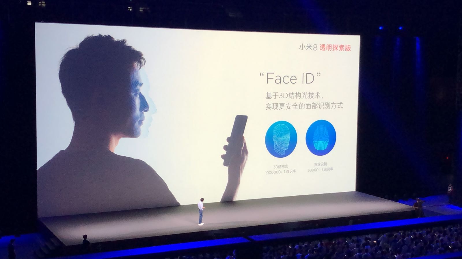
Xiomi's new Mi8 Explorer Edition flagship device is said to be the world's first Android device with integrated 3D imaging and scanning capabilities. The 3D camera will allow 3D face scanning and recognition, face 3D capturing for a secure ePayment, and will enable AR features both for end users as well as for developers.

Mantis Vision's technology is based on structured light and a smart decoding algorithm. According to Gur Arie Bittan, founder and CEO of Mantis Vision: "Shrink optical stack and size from centimeters to millimeters, incorporate Vcel lasers that were still nascent technologies at the time, meet OEM's power consumption drastic points and conform with eye safety regulations, build camera brackets module that synchronizes with RGB existing cameras, define and prepare for mass production calibration and on software invent effective decoding patters algorithms and pipelines running on one Arm Core on the AP. Mantis Vision Teams overcame the many challenges they were confronted and succeeded build the most cost-effective 3D Structure Light camera module there is on the market today while using Mantis Vision in-house IP's."

Few pictures from today's Xiaomi presentation (sorry, I can't translate Chinese):

ADI Talks about its LiDAR for the First Time

SeekingAlpha transcript of Analog Devices earnings call has an interesting mention about the company's LiDAR development:

"If turn to autonomous vehicles, we haven’t really talked much before about our LIDAR solution, but we’re gaining design-ins today in long and short range, LIDAR systems with both the ADI mix signal technologies and the LT portfolios, and even getting some sockets for Hittite in the very, very high frequency areas. And these components compliment the more advanced capability that we’re working on now to produce a solid-state beam steering and photo-detector technology.

And that will dramatically drive the size, the cost, the power and we believe enable over the longer term that is the kind of mid to long-term 3, 4, 5 years mass deployment of LIDAR and we’ve got that new technology in terms of that more integrated system capability through the acquisition of Vescent sometime last year.
"

Wednesday, May 30, 2018

Sony Dual Selfie Camera

Sony Mobile publishes an article on its Dual Selfie camera in Xperia XA2 Ultra smartphone:

"The Dual Selfie Camera offers the standard 80 degree lens for close ups, alongside a super wide 120 degree lens for wider images, giving you the best of both worlds. An added benefit is, with the wider lens, there’s no need for a selfie stick, even if you’re trying to fit a bunch of friends into frame.

...our lens design technology has improved. A wider FOV (Field of View) lens would normally create distortion but the lens design of the 120 degree camera for XA2 Ultra was designed to reduce such warping.

I can’t say too much, but selfie enabled AI may be on it’s way. We’re developing the next generation camera experience – it’s exciting stuff.
"

Tuesday, May 29, 2018

Etron Has High Hopes for its 3D Solution

Digitimes: Etron 3D wide-angle sensor-based face recognition modules adopted by Ant Financial, the online payment arm of e-commerce giant Alibaba Group, at its first unmanned store in Hangzhou, China, a move that is expected to significantly improve Etrons's revenue and profits.

The company's EX8036 3D multi-aperture measurement/gesture recognition system is based on a 3D AI-vision IC/ platform with a wide range of distant detection from 20cm to 3.5m, with field view angle up to 114 degrees. It can provide clear images even in environments with a luminosity of only 4 lumens.

The company chairman Nicky Lu expects good business prospects for the 3D sensor-based recognition modules, given the proliferation of self-service stores in China and the US.

After Kickstarter Success, SiOnyx Continues on Indiegogo

After the Kickstarter crowdfunding campaign, SiOnyx starts another one on Indiegogo:

GPixel and TowerJazz Announce Prototypes of 2.5um Global Shutter Pixel Sensor

Globenewswire: TowerJazz and Gpixel announce a Gpixel's GMAX0505, a 25MP sensor based on TowerJazz's 2.5um global shutter pixel in a 1.1" optical format with the highest resolution in C-mount optics. This type of lens mount is commonly found in closed-circuit television cameras, machine vision and scientific cameras.

TowerJazz's 2.5um GS pixel is said to be the smallest in the world; the otherwise currently available smallest pixel for such high-end applications used in the market is 3.2um (65% larger) and demonstrates overall lower performance. TowerJazz's 2.5um global shutter pixel features a unique light pipe technology, great angular response, more than 80dB shutter efficiency in spite of the extreme small size, and extremely low noise of 1e-. Gpixel has started prototyping its GMAX0505 using TowerJazz's 65nm process on a 300mm platform in its Uozu, Japan facility.

"TowerJazz has been an important and strategic fab partner of Gpixel for many years. We are very pleased with the support of great technology innovation from TowerJazz with our current global shutter sensor families, backside illuminated scientific CMOS sensor solutions and today, the next generation global shutter industrial sensor product family," said Xinyang Wang, CEO of Gpixel, Inc. "The GMAX0505 is our second product after our first 2.8um pixel product that is already ramped up into production at TowerJazz's Arai fab in Japan. We are very excited and looking forward to seeing more products using this pixel technology in the near future. The successful introduction of the new 25Mp product will bring our customers a unique advantage in the growing demand of machine vision applications."

Avi Strum, TowerJazz Senior VP and GM of CMOS Image Sensor Business Unit, said, "We are very excited to be the first and only foundry in the world to offer this new technology - the smallest global shutter pixel available. Through our collaboration with Gpixel, we are able to create a compact package design which allows for miniature camera design. We are pleased with our long term relationship with Gpixel and with the way our technology combined with their excellent products allow us to target and gain market share in the growing high resolution industrial markets."

GMAX0505 is a charge domain global shutter image sensor which has 70% peak QE and can run up to 150fps frame rate.

Monday, May 28, 2018

Yole on ON Semi Leadership in Automotive Imaging

Yole article "ON Semiconductor is the new king of the road for image sensors" states that ON Semiconductor automotive image sensor sales are growing. Yole estimates that they accounted for 48% of the imaging division’s $768M sales in 2017.

LFoundry Avezzano, Italy, fab wafer production should be in the range of 100,000 8” wafers per year for its key customer, while the fab’s capacity is 160,000 wafers per year. ON Semi has actually grown its automotive image sensor business at a 55% compound annual growth rate (CAGR) in the last six years. ADAS is only one fifth of the story, as ON Semi’s sensors also ended up in automotive ‘surround cameras’.

Imasenic on Way to Gfps Image Sensors

Workshop on Computational Image Sensors and Smart Cameras held in May 2017 in Barcelona, Spain publishes Renato Turchetta's presentation "Towards Gfps CMOS image sensors:"

Energias Market Research on CIS Market

Energias Market Research expects the image sensor market to grow significantly from $14.1b in 2017 to $25.6b in 2024 at a CAGR of 10.3%. However, high manufacturing cost may hamper the growth of the market.

"3D image sensor is a fastest growing market due to growing applications in computer vision and machine vision. On the basis of spectrum, non-visible spectrum is anticipated to grow with a highest CAGR owing to increasing usage in medical, automotive, consumer electronics and industrial applications. Based on application, consumer electronics segment is expected to account for highest market share in image sensor market."

Sunday, May 27, 2018

Pixart Q1 2018 Report

Pixart Q1 2018 report shows that despite its diversification efforts, the company remains mainly an optical mouse sensors provider:

Saturday, May 26, 2018

ESA Pays $47M to e2v to Supply 114 CCDs for Plato Mission

The European Space Agency (ESA) has awarded Teledyne e2v with the second phase of a €42M ($47M) contract to produce visible light CCDs for the PLATO (Planetary Transits and Oscillations of stars) mission. PLATO is a planet hunting spacecraft that will seek out and research Earth like exoplanets around Sun like stars.

Teledyne e2v completed the first manufacturing phase of the contract, including the production of CCD wafers and the procurement and production of other key items. After a successful review of the first phase, Teledyne e2v has been authorised to start work on phase two of this prestigious contract. This includes manufacturing the wafers and the assembly, test and delivery of 114 CCDs. Together, they will form the biggest optical array ever to be launched into space (currently planned for 2026).

PLATO will be made up of 26 telescopes mounted on a single satellite platform. Each telescope will contain four 20MP Teledyne e2v CCDs in both full-frame and frame-transfer variants, for a full satellite total of 2.12 Gpixels. This is over twice the equivalent number for GAIA, the largest camera currently in space. As with GAIA, all of the PLATO CCD image sensors will be designed and produced in Chelmsford, UK.

Friday, May 25, 2018

Pulse-Based ToF Sensing

MPDI Special Issue Depth Sensors and 3D Vision publishes University of Siegen, Germany, paper "Pulse Based Time-of-Flight Range Sensing" by Hamed Sarbolandi, Markus Plack, and Andreas Kolb.

"Pulse-based Time-of-Flight (PB-ToF) cameras are an attractive alternative range imaging approach, compared to the widely commercialized Amplitude Modulated Continuous-Wave Time-of-Flight (AMCW-ToF) approach. This paper presents an in-depth evaluation of a PB-ToF camera prototype based on the Hamamatsu area sensor S11963-01CR. We evaluate different ToF-related effects, i.e., temperature drift, systematic error, depth inhomogeneity, multi-path effects, and motion artefacts. Furthermore, we evaluate the systematic error of the system in more detail, and introduce novel concepts to improve the quality of range measurements by modifying the mode of operation of the PB-ToF camera. Finally, we describe the means of measuring the gate response of the PB-ToF sensor and using this information for PB-ToF sensor simulation."

Olympus Multi-Storied Photodiode Sensor

MDPI Special Issue Special Issue on the 2017 International Image Sensor Workshop (IISW) publishes Olympus paper "Multiband Imaging CMOS Image Sensor with Multi-Storied Photodiode Structure" Yoshiaki Takemoto, Mitsuhiro Tsukimura, Hideki Kato, Shunsuke Suzuki, Jun Aoki, Toru Kondo, Haruhisa Saito, Yuichi Gomi, Seisuke Matsuda, and Yoshitaka Tadaki.

"We developed a multiband imaging CMOS image sensor (CIS) with a multi-storied photodiode structure, which comprises two photodiode (PD) arrays that capture two different images, visible red, green, and blue (RGB) and near infrared (NIR) images at the same time. The sensor enables us to capture a wide variety of multiband images which is not limited to conventional visible RGB images taken with a Bayer filter or to invisible NIR images. Its wiring layers between two PD arrays can have an optically optimized effect by modifying its material and thickness on the bottom PD array. The incident light angle on the bottom PD depends on the thickness and structure of the wiring and bonding layer, and the structure can act as an optical filter. Its wide-range sensitivity and optimized optical filtering structure enable us to create the images of specific bands of light waves in addition to visible RGB images without designated pixels for IR among same pixel arrays without additional optical components. Our sensor will push the envelope of capturing a wide variety of multiband images."

Concept of multi-storied photodiode CMOS sensor based on 3D stacked technology. There are two layers of PD arrays, one in the top and the other in the bottom semiconductor. The top PD array converts a part of incident light into signals and works as an optical filter for the bottom PD array. The bottom PD array converts light that penetrates through the top substrate into signals, which means the top substrate acts mainly as a visible light sensor and the bottom one is an invisible IR light sensor.

Black Phosphorus NIR Photodetectors

MDPI Sensors publishes a paper "Multilayer Black Phosphorus Near-Infrared Photodetectors" by Chaojian Hou, Lijun Yang, Bo Li, Qihan Zhang, Yuefeng Li, Qiuyang Yue, Yang Wang, Zhan Yang, and Lixin Dong from Harbin Institute of Technology (China), Michigan State University (USA), and Soochow University (China).

"Black phosphorus (BP), owing to its distinguished properties, has become one of the most competitive candidates for photodetectors. However, there has been little attention paid on photo-response performance of multilayer BP nanoflakes with large layer thickness. In fact, multilayer BP nanoflakes with large layer thickness have greater potential from the fabrication viewpoint as well as due to the physical properties than single or few layer ones. In this report, the thickness-dependence of the intrinsic property of BP photodetectors in the dark was initially investigated. Then the photo-response performance (including responsivity, photo-gain, photo-switching time, noise equivalent power, and specific detectivity) of BP photodetectors with relative thicker thickness was explored under a near-infrared laser beam (λIR = 830 nm). Our experimental results reveal the impact of BP’s thickness on the current intensity of the channel and show degenerated p-type BP is beneficial for larger current intensity. More importantly, the photo-response of our thicker BP photodetectors exhibited a larger responsivity up to 2.42 A/W than the few-layer ones and a fast response photo-switching speed (response time is ~2.5 ms) comparable to thinner BP nanoflakes was obtained, indicating BP nanoflakes with larger layer thickness are also promising for application for ultra-fast and ultra-high near-infrared photodetectors."

Unfortunately, no spectrum response of QE measurements are published. The EQE at 830nm graphs show large internal gain of photosensitive FET structures:

Thursday, May 24, 2018

AEye Introduces Dynamic Vixels

PRNewswire: AEye introduces a new sensor data type called Dynamic Vixels. In simple terms, Dynamic Vixels combine pixels from digital 2D cameras with voxels from AEye's Agile 3D LiDAR sensor into a single super-resolution sensor data type.

"There is an ongoing argument about whether camera-based vision systems or LiDAR-based sensor systems are better," said Luis Dussan, Founder and CEO of AEye. "Our answer is that both are required – they complement each other and provide a more complete sensor array for artificial perception systems. We know from experience that when you fuse a camera and LiDAR mechanically at the sensor, the integration delivers data faster, more efficiently and more accurately than trying to register and align pixels and voxels in post-processing. The difference is significantly better performance."

"There are three best practices we have adopted at AEye," said Blair LaCorte, Chief of Staff. "First: never miss anything; second: not all objects are equal; and third: speed matters. Dynamic Vixels enables iDAR to acquire a target faster, assess a target more accurately and completely, and track a target more efficiently – at ranges of greater than 230m with 10% reflectivity."

Qualcomm Snapdragon 710 Supports 6 Cameras, ToF Sensing, More

Qualcomm 10nm Snapdragon 710 processors features a number of advanced imaging features:
  • Qualcomm Spectra 250 ISP
  • 2nd Generation Spectra architecture
  • 14-bit image signal processing
  • Up to 32MP single camera
  • Up to 20MP dual camera
  • Can connect up to 6 different cameras (many configurations possible)
  • Multi-Frame Noise Reduction (MFNR) with accelerated image stabilization
  • Hybrid Autofocus with support for dual phase detection (2PD) sensors
  • Ultra HD video capture (4K at 30 fps) with Motion Compensated Temporal Filtering (MCTF)
  • Takes 4K Ultra HD video at up to 40% lower power
  • 3D structured light and time of flight active depth sensing

Mobileye Autonomous Car Fails in Demo

EETimes Junko Yoshida publishes an explanation of Mobileye self-driving car demo where the car passes a junction on red light:

"The public AV demo in Jerusalem inadvertently allowed a local TV station’s video camera to capture Mobileye’s car running a red light. (Fast-forward the video to 4:28 for said scene.)

According to Mobileye, the incident was not a software bug in the car. Instead, it was triggered by electromagnetic interference (EMI) between a wireless camera used by the TV crew and the traffic light’s wireless transponder. Mobileye had equipped the traffic light with a wireless transponder — for extra safety — on the route that the AV was scheduled to drive in the demo. As a result, crossed signals from the two wireless sources befuddled the car. The AV actually slowed down at the sight of a red light, but then zipped on through.
"


On a similar theme, NTSB publishes a preliminary analysis of Uber self-driving car crash that killed a women in Arizona in March 2018:

According to data obtained from the self-driving system, the system first registered radar and LIDAR observations of the pedestrian about 6 seconds before impact, when the vehicle was traveling at 43 mph. As the vehicle and pedestrian paths converged, the self-driving system software classified the pedestrian as an unknown object, as a vehicle, and then as a bicycle with varying expectations of future travel path. At 1.3 seconds before impact, the self-driving system determined that an emergency braking maneuver was needed to mitigate a collision. According to Uber, emergency braking maneuvers are not enabled while the vehicle is under computer control, to reduce the potential for erratic vehicle behavior. The vehicle operator is relied on to intervene and take action. The system is not designed to alert the operator.

SystemPlus on iPhone X Color Sensor

SystemPlus reverse engineering shows a difference between iPhone X color sensors and other AMS spectral sensors:

Wednesday, May 23, 2018

Nice Animations

Lucid Vision Labs publishes nice animations explaining how Sony readout with dual analog/digital CDS works:

Sony Exmor rolling shutter sensor
Same pipeline but with global shutter (Pregius)
1st stage - analog domain CDS
2nd stage - digital domain CDS

There are few more animations on the company's site and also a pictorial image sensor tutorial.

Tuesday, May 22, 2018

NHK Presents 8K Selenium Sensor

NHK Open House to be held on May 24-27 exhibits an 8K avalanche-multiplying crystalline selenium image sensor:

"Electric charge generated by incident light are increased by avalanche multiplication phenomenon inside the photoelectric conversion film. The film can be overlaid on a CMOS circuit with a low breakdown voltage because avalanche multiplication occurs at low voltage in crystalline selenium, which can absorb a sufficient amount of light even when thin."

The paper on crystalline selenium-based image sensor has been published in 2015.

Pixelligent Raises $7.6M for Nanoparticle Microlens

BusinessWire: Baltimore, MD-based Pixelligent's Zirconium oxide capped nanoparticles (ZrO2), a high refractive index inorganic material, with a sub-10 nm diameter with functionalized surface, is said to have a potential to contribute to sensitivity of CMOS image sensors. The company announces $7.6M in new funding to help further drive product commercialization and accelerate global customer adoption.

Although Pixelligent lenses for image sensor applications have been announced a couple of years ago, there is no such product on the market yet, to the best of my knowledge. In 2013, the company President & CEO Craig Bandes said: "During the past 12 months we have seen a tremendous increase in demand for our nanocrystal dispersions spanning the CMOS Image Sensor, ITO, LED, OLED and Flat Panel Display markets. This demand is coming from customers around the globe with the fastest growth being realized in Asia. In the first quarter of 2013, we began shipping our first commercial orders and currently have more than 30 customers at various stages of product qualification."

Sony Image Sensor Business Strategy

Sony IR Day 2018 held on May 22 (today) has quite a detailed presentation on its semiconductor business targets and strategy. From the Sony official PR:

"In the area of CMOS image sensors that capture the real world in which we all live, and are vital to KANDO content creation, aim to maintain Sony’s global number one position in imaging applications, and become the global leader in sensing.

Through the key themes of KANDO - to move people emotionally - and "getting closer to people," Sony will aim to sustainably generate societal value and high profitability across its three primary business areas of electronics, entertainment, and financial services. It will pursue this strategy based on the following basic principles.

CMOS image sensors are key component devices in growth industries such as the Internet of Things, artificial intelligence, autonomous vehicles, and more. Sony's competitive strength in this area is based on its wealth of technological expertise in analog semiconductors, cultivated over many years from the charge-coupled device (CCD) era. Sony aims to maintain its global number one position in imaging and in the longer term become the number one in sensing applications. To this end, Sony will extend its development of sensing applications beyond the area of smartphones, into new domains such as automotive use.

...based on its desire to contribute to safety in the self-driving car era, Sony will work to further develop its imaging and sensing technologies.
"

Monday, May 21, 2018

Hamamatsu Sensors in Automotive Applications

Hamamatsu publishes a nice article "Photonics for advanced car technologies" showing many applications for its light sensors: