Photron publishes nice videos shot by its Crysta polarization camera:
Sunday, March 31, 2019
Saturday, March 30, 2019
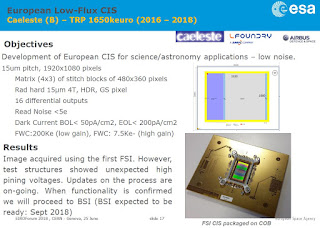
ESA Investments in CIS Technology
Caeleste publishes a link to slides on European Space Agency programs and budgets on image sensor technology development. Some of the projects are successful, others end with failures:


Friday, March 29, 2019
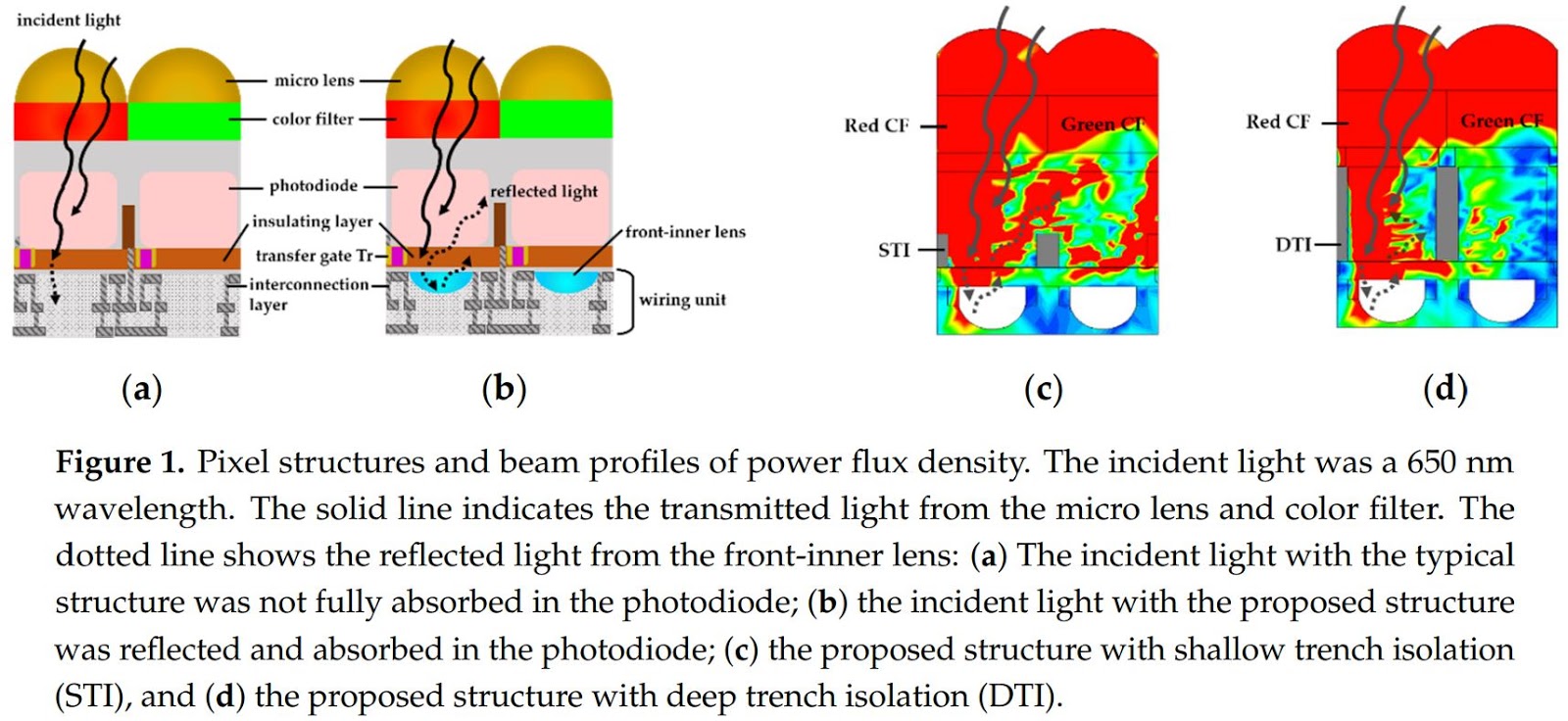
Front Side Microlens for BSI Pixel
MDPI paper "Front-Inner Lens for High Sensitivity of CMOS Image Sensors" by Godeun Seok and Yunkyung Kim from Dong-A University, Busan, Korea propose dual-side microlens for small pixels:
"Due to the continuing improvements in camera technology, a high-resolution CMOS image sensor is required. However, a high-resolution camera requires that the pixel pitch is smaller than 1.0 μm in the limited sensor area. Accordingly, the optical performance of the pixel deteriorates with the aspect ratio. If the pixel depth is shallow, the aspect ratio is enhanced. Also, optical performance can improve if the sensitivity in the long wavelengths is guaranteed. In this current work, we propose a front-inner lens structure that enhances the sensitivity to the small pixel size and the shallow pixel depth. The front-inner lens was located on the front side of the backside illuminated pixel for enhancement of the absorption. The proposed structures in the 1.0 μm pixel pitch were investigated with 3D optical simulation. The pixel depths were 3.0, 2.0, and 1.0 μm. The materials of the front-inner lens were varied, including air and magnesium fluoride (MgF2). For analysis of the sensitivity enhancement, we compared the typical pixel with the suggested pixel and confirmed that the absorption rate of the suggested pixel was improved by a maximum of 7.27%, 10.47%, and 29.28% for 3.0, 2.0, and 1.0 μm pixel depths, respectively."


"Due to the continuing improvements in camera technology, a high-resolution CMOS image sensor is required. However, a high-resolution camera requires that the pixel pitch is smaller than 1.0 μm in the limited sensor area. Accordingly, the optical performance of the pixel deteriorates with the aspect ratio. If the pixel depth is shallow, the aspect ratio is enhanced. Also, optical performance can improve if the sensitivity in the long wavelengths is guaranteed. In this current work, we propose a front-inner lens structure that enhances the sensitivity to the small pixel size and the shallow pixel depth. The front-inner lens was located on the front side of the backside illuminated pixel for enhancement of the absorption. The proposed structures in the 1.0 μm pixel pitch were investigated with 3D optical simulation. The pixel depths were 3.0, 2.0, and 1.0 μm. The materials of the front-inner lens were varied, including air and magnesium fluoride (MgF2). For analysis of the sensitivity enhancement, we compared the typical pixel with the suggested pixel and confirmed that the absorption rate of the suggested pixel was improved by a maximum of 7.27%, 10.47%, and 29.28% for 3.0, 2.0, and 1.0 μm pixel depths, respectively."


Collabo Innovations vs Sony Appeal Oral Argument Recording
For those who are curious how the US court arguments sound like, can listen to an mp3 recording of Collabo Innovations vs Sony case appeal held on March 5, 2019:
The patents in this lawsuit are US5,952,714 "Solid-state image sensing apparatus and manufacturing method thereof" and US8,030,724 "Solid-state imaging device and method for fabricating the same." Collabo acquired both of them from Panasonic.
The patents in this lawsuit are US5,952,714 "Solid-state image sensing apparatus and manufacturing method thereof" and US8,030,724 "Solid-state imaging device and method for fabricating the same." Collabo acquired both of them from Panasonic.
Prophesee Invests in Software
Prophesee releases a driver for Robot Operating System (ROS).
The company also publishes an arxiv.org paper "Speed Invariant Time Surface for Learning to Detect Corner Points with Event-Based Cameras" by Jacques Manderscheid, Amos Sironi, Nicolas Bourdis, Davide Migliore, and Vincent Lepetit.
"We propose a learning approach to corner detection for event-based cameras that is stable even under fast and abrupt motions. Event-based cameras offer high temporal resolution, power efficiency, and high dynamic range. However, the properties of event-based data are very different compared to standard intensity images, and simple extensions of corner detection methods designed for these images do not perform well on event-based data. We first introduce an efficient way to compute a time surface that is invariant to the speed of the objects. We then show that we can train a Random Forest to recognize events generated by a moving corner from our time surface. Random Forests are also extremely efficient, and therefore a good choice to deal with the high capture frequency of event-based cameras ---our implementation processes up to 1.6Mev/s on a single CPU. Thanks to our time surface formulation and this learning approach, our method is significantly more robust to abrupt changes of direction of the corners compared to previous ones. Our method also naturally assigns a confidence score for the corners, which can be useful for postprocessing. Moreover, we introduce a high-resolution dataset suitable for quantitative evaluation and comparison of corner detection methods for event-based cameras. We call our approach SILC, for Speed Invariant Learned Corners, and compare it to the state-of-the-art with extensive experiments, showing better performance."

Thanks to TL for the pointer!
Thursday, March 28, 2019
SPAD-based LiDAR in Bright Sunlight
A group of researches from University of Wisconsin-Madison publishes a nice arxiv.org paper analyzing SPAD LiDAR performance in bright sunlight: "Photon-Flooded Single-Photon 3D Cameras" by Anant Gupta, Atul Ingle, Andreas Velten, and Mohit Gupta:
"Single photon avalanche diodes (SPADs) are starting to play a pivotal role in the development of photon-efficient, long-range LiDAR systems. However, due to non-linearities in their image formation model, a high photon flux (e.g., due to strong sunlight) leads to distortion of the incident temporal waveform, and potentially, large depth errors. Operating SPADs in low flux regimes can mitigate these distortions, but, often requires attenuating the signal and thus, results in low signal-to-noise ratio. In this paper, we address the following basic question: what is the optimal photon flux that a SPAD-based LiDAR should be operated in? We derive a closed form expression for the optimal flux, which is quasi-depth-invariant, and depends on the ambient light strength. The optimal flux is lower than what a SPAD typically measures in real world scenarios, but surprisingly, considerably higher than what is conventionally suggested for avoiding distortions. We propose a simple, adaptive approach for achieving the optimal flux by attenuating incident flux based on an estimate of ambient light strength. Using extensive simulations and a hardware prototype, we show that the optimal flux criterion holds for several depth estimators, under a wide range of illumination conditions."


"Single photon avalanche diodes (SPADs) are starting to play a pivotal role in the development of photon-efficient, long-range LiDAR systems. However, due to non-linearities in their image formation model, a high photon flux (e.g., due to strong sunlight) leads to distortion of the incident temporal waveform, and potentially, large depth errors. Operating SPADs in low flux regimes can mitigate these distortions, but, often requires attenuating the signal and thus, results in low signal-to-noise ratio. In this paper, we address the following basic question: what is the optimal photon flux that a SPAD-based LiDAR should be operated in? We derive a closed form expression for the optimal flux, which is quasi-depth-invariant, and depends on the ambient light strength. The optimal flux is lower than what a SPAD typically measures in real world scenarios, but surprisingly, considerably higher than what is conventionally suggested for avoiding distortions. We propose a simple, adaptive approach for achieving the optimal flux by attenuating incident flux based on an estimate of ambient light strength. Using extensive simulations and a hardware prototype, we show that the optimal flux criterion holds for several depth estimators, under a wide range of illumination conditions."


e2v Announces Another 5MP GS Sensor
Globenewswire: Following 5MP sensor in Emerald family, Teledyne e2v adds a new 5MP GS sensor in its Snappy family for barcode reading, 2D scanning and other applications. Available in both monochrome and color, the Snappy 5M has a 1/1.8 inch optical format, containing a 2.8 μm global shutter pixel and able to output video at ~50 fps at 10 bits over a 4 wire, MIPI CSI-2 interface.
Snappy 5M is designed to enable fast, extended range scanning and includes powerful unique patented features and region of interest modes:

Snappy 5M is designed to enable fast, extended range scanning and includes powerful unique patented features and region of interest modes:
- A Fast Self Exposure (FSE) mode automatically calculates the optimum integration time that is applied to the first image from the device. The mode is user programmable and provides continuous fast decoding, tolerating any kind of lighting or dynamic lighting environment. This is advantageous compared with conventional auto exposure methods, improving convergence speed and robustness.
- A Smart ROI feature searches for barcodes in the image frame, and reports their locations as metadata in the image footer. The regions of the image containing barcodes are discerned from the background image to considerably reduce downstream image processing (FPGA/CPU/DSP) power, time and cost. Up to 16 different regions can be detected simultaneously. Other forms of repetitive signatures such as printed character strings can also be detected for document scanning and OCR applications.

Yole on LiDAR Market
Yole Developpement publishes a report "LiDAR for Automotive and Industrial Applications 2019." Few quotes:
"The total LiDAR market was worth $1.3B in 2018 and is expected to reach $6B by 2024. Automotive applications should represent 70% of the total market.
Huge investments have been made since 2016, surpassing $1B and showing the great interest in LiDAR technology and more generally autonomous driving features. MEMS is the technology attracting most investments, followed by optical phased arrays, although investments in the latter have considerably declined since 2016.
Therefore, MEMS and flash technologies seem to be favored by LiDAR manufacturers. These two technologies are promising and should be introduced rapidly into the market: MEMS will be introduced by BMW in 2021; flash is being pushed by Continental, expecting an introduction by a carmaker in 2020.
A majority of LiDAR manufacturers are using optical components at a wavelength of 905nm due to their large availability at a reasonable cost compared with 1550nm components. Edge emitting lasers and avalanche photodiodes at 905nm are typical components of LiDARs developed today. Other components like vertical cavity surface emitting lasers (VCSELs), single-photon avalanche diodes (SPADs), and silicon photomultipliers (SiPMs) can also be used. However, they are expected in the next generation of LiDAR, as time is needed to increase their performance and reduce their cost."


Wednesday, March 27, 2019
Huawei P30 Pro Gets Highest DxOMark, Uses RYYB CFA in Main Sensor and Dedicated ToF Sensor
Huawei new flagship smartphone, P30 Pro wins the highest DxOMark for its camera:

The most interesting fact is that such a high score has been achieved with RYYB color filter pattern in its main sensor. Aptina has patented that pattern several years ago. It's not immediately clear whether Huawei or its CIS supplier have licensed this patent or found a way around it.


Thanks to TS for the pointer!
Update: Few more pictures from Huawei presentation:


Emmy Award for Color Filter Technology
Globenewswire: Peter Dillon and Albert Brault will receive Technology Emmy Awards from the National Academy of Television Arts & Sciences for their “Pioneering Development of the Single-Chip Color Camera” on April 7th in Las Vegas, NV. Their inventions include coating a mosaic of color filters over the light sensitive pixels on an image sensor and developing demosaicing algorithms to generate color video images. This technology is widely used to produce television programs and movies. It’s also used to create color photos and video clips in a broad range of products, including smart phone cameras, drones, and medical imaging devices.
Peter Dillon said “We’re delighted to receive this recognition for our research. We’d like to thank all our team members, who helped us develop and demonstrate the world’s first integral color image sensors and cameras. It’s amazing what a revolution this has created in how people around the world use color images to communicate.”
Albert Brault said “By combining my knowledge of chemistry with Peter’s understanding of solid-state electronics, we created a new way of sensing color images. We were fortunate to have all the support and infrastructure needed to turn our ideas into working devices. Decades later, we’re thrilled that Rochester remains the world’s center for photonics and imaging.”
In early 1974, while at Kodak Research Labs (KRL), Dillon lead a team developing an early prototype color video camcorder. Instead of the conventional design using a large color prism and three CCD sensors, he conceived the idea of fabricating a color filter mosaic over the individual pixels of a single CCD. Brault, his KRL colleague, then perfected a process for coating organic color dyes through photoresist windows during wafer fabrication. To determine the optimum color pattern, Peter consulted KRL mathematician Bryce Bayer, who invented the checkerboard arrangement now known as the “Bayer Pattern”. These visionary ideas made capturing color digital images inexpensive and ubiquitous. Today, nearly everyone carries the technology they developed in their purse or pocket, since billions of integral color sensors are used each year in smart phones.
Dillon presented a paper, co-authored by Brault, describing the world's first single-chip color sensor in December 1976 at IEDM in Washington D.C. The auditorium was packed with scientists from the leading semiconductor and video camera manufacturers. Afterwards, many visited KRL to learn about this important imaging breakthrough.
The research building where Dillon and Brault worked was expanded in the early 1980s to manufacture the world’s first color megapixel imagers, which were used in many pioneering digital cameras. The facility is used today by ON Semiconductor to fabricate color CCDs with up to 50MP.
 |
| First Color CCD image sensor |
 |
| First single-chip color camera |

Ouster Reports 400 Customers, Raises $60M
PRNewswire: LiDAR startup Ouster announces it has a roster of over 400 customers and the addition of over $60M in funding. The company also opens of a new manufacturing facility in San Francisco producing hundreds of LiDARs per month and capable of producing thousands of LiDARs per month toward the end of 2019. Transparent pricing and short 2-3 week lead times for sensor delivery are claimed to help the company stand out in a crowded market.
The additional $60M in equity and debt funding includes investments from Runway Growth Capital and Silicon Valley Bank, as well as additional funding from Series A participants Cox Enterprises, Constellation Tech Ventures, Fontinalis Partners, Carthona, and others.
Since Ouster launched in late 2017, the company has announced 4 LiDARs with resolutions from 16 to 128 channels, as well as two product lines: the OS-1 and OS-2. What started as a 4-person team working in a tiny warehouse three years ago has grown to over 100 full-time employees across engineering, operations, business development, and marketing. The company expects to nearly double its headcount in the coming year to support further product line development and meet the global demand for its high-resolution LiDARs.
Update: In comparison, Velodyne claims "only" 250 customers so far.
Tuesday, March 26, 2019
Teledyne e2v Releases 4MP BSI Rad-Hard Sensor
Teledyne e2v has released a new image sensor, the CIS120, for harsh environments such as space applications. Samples have been available since February 2019 along with a full test and demonstration system.
Key specifications of the CIS120 include a resolution of 2048 x 2048 and BSI 10µm square pixels with a QE of 90% at 550 nm (typical). The sensor offers both a rolling shutter mode with a frame rate of 30 fps (8 bit) and a global shutter mode with a frame rate of 20 fps (12 bit).
Key features include:
- Good latch-up immunity and high SEU threshold by design and is resistant to ionising radiation by process choice
- Pixel read timing is set by an on-chip sequencer to simplify use and to reduce pin count
- A column parallel ADC is controlled by its own sequencer
- Resolution can be set anywhere from 8 to 14 bits
- Four LVDS channels output the image data and are controlled by the readout sequencer to scan along each row in turn.
- All configuration settings are programmed over an SPI. This includes shutter mode, ADC resolution and bias current values
- Package options include ceramic PGA and metal and ceramic three-side butting designs for use in mosaic focal planes
- CIS120 is stitched, so other sizes are possible from 2048 × 1024, up to 2048 × 8192 pixels, without the cost of new masks as well as other customer-specific requirements such as anti-reflective coatings
- An increased charge capacity of 100 ke– is possible by a metal pattern change


Innoviz Raises $132M More
PRNewswire: LiDAR startup Innoviz has raised $132M in Series C funding. The round is marked by the entrance of new major investors China Merchants Capital, Shenzhen Capital Group and New Alliance Capital; Harel Insurance Investments and Financial Services and Phoenix Insurance Company. Given demand from additional investors, the Series C round will remain open for a second closing to be announced in the coming months.
The new round will support Innoviz's commercialization of InnovizPro and InnovizOne LiDARs. A partnership with Magna International, which also participated in the round, resulted in Innoviz's automotive-grade LiDAR, InnovizOne, and its computer vision software being selected by BMW for series production of vehicles starting in 2021.
"We've experienced significant growth over the past year to meet increased demand for solid-state LiDAR. This fundraising enables many of the substantial commitments it takes to bring this technology to market at a massive scale — the scale required by Tier 1 suppliers and automakers leveraging LiDAR to deliver autonomous vehicles to the masses by 2021. We're excited to transition our production, manufacturing and research and development efforts into the next phase and continue to furnish the full stack of LiDAR hardware and software solutions to the industry," said Omer Keilaf, CEO and co-founder of Innoviz. "This round is a strong testament to the excellent progress we've made in cementing our technology as a true market leader capable of meeting the rigorous automotive standards at a cost that makes mass production realistic."


TPSCo Extends CIS Supply Agreement with Panasonic through 2022
GlobeNewswire: TowerJazz and TowerJazz Panasonic Semiconductor Company (TPSCo) announced they have signed a three-year agreement, extending its previous business partnership with Panasonic through 2022. Under the agreement, Panasonic will continue to utilize TPSCo three manufacturing facilities in Japan for its semiconductor business. Wafer loading level from PSCS to TPSCo fabs is expected to remain similar, with a new pricing structure, resulting in revenue reductions of approximately $20m per quarter, with revenue and margins targeted to be compensated through presently implemented efficiencies and cost reduction activities, as well as third party revenue growth, including the present strong 300mm utilization ramp.
Through TPSCo, TowerJazz offers its customers 300mm manufacturing platforms such as 65nm CIS. TowerJazz to maintain its 51% holding of TPSCo shares, with Panasonic as a 49% shareholder.
Through TPSCo, TowerJazz offers its customers 300mm manufacturing platforms such as 65nm CIS. TowerJazz to maintain its 51% holding of TPSCo shares, with Panasonic as a 49% shareholder.
Monday, March 25, 2019
SPAD Imagers in Biophotonics Review
Arxiv.org paper "Single-photon SPAD imagers in biophotonics: Review and Outlook" by Claudio Bruschini, Harald Homulle, Ivan Michel Antolovic, Samuel Burri, and Edoardo Charbon from EPFL and TU Delft presents an excellent overview of the recent advances in the field:
"Single-photon avalanche diode (SPAD) arrays are solid-state detectors offering imaging capabilities at the level of individual photons, with unparalleled photon counting and time-resolved performance. This fascinating technology has progressed at very high pace in the past 15~years, since its inception in standard CMOS technology in 2003. A host of architectures has been explored, ranging from simpler implementations, based solely on off-chip data processing, to progressively "smarter" sensors including on-chip, or even pixel-level, timestamping and processing capabilities. As the technology matured, a range of biophotonics applications has been explored, including (endoscopic) FLIM, (multi-beam multiphoton) FLIM-FRET, SPIM-FCS, super-resolution microscopy, time-resolved Raman, NIROT, and PET. We will review some representative sensors and their corresponding applications, including the most relevant challenges faced by chip designers and end-users. Finally, we will provide an outlook on the future of this fascinating technology."
"Single-photon avalanche diode (SPAD) arrays are solid-state detectors offering imaging capabilities at the level of individual photons, with unparalleled photon counting and time-resolved performance. This fascinating technology has progressed at very high pace in the past 15~years, since its inception in standard CMOS technology in 2003. A host of architectures has been explored, ranging from simpler implementations, based solely on off-chip data processing, to progressively "smarter" sensors including on-chip, or even pixel-level, timestamping and processing capabilities. As the technology matured, a range of biophotonics applications has been explored, including (endoscopic) FLIM, (multi-beam multiphoton) FLIM-FRET, SPIM-FCS, super-resolution microscopy, time-resolved Raman, NIROT, and PET. We will review some representative sensors and their corresponding applications, including the most relevant challenges faced by chip designers and end-users. Finally, we will provide an outlook on the future of this fascinating technology."

Sunday, March 24, 2019
Credit Suisse on Smartphone CIS Market: 108MP and 64MP Sensors are Coming
IFNews: Credit Suisse update dated by March 13, 2019, reports on CIS market:
"We note a sustained shift toward higher image resolution and multi-camera imaging systems in CIS. In Oct–Dec 2018, the multi-camera adoption rate fell briefly to 43% due to a slump in Apple’s dual-camera-equipped OLED models (vs. 65% in Jul–Sep and 58% in Oct–Dec 2017). However, we note the trend accelerating in non-Apple Android devices with 52% (43%, 21%). The multi-camera system adoption rate across smartphones finished at 40% in 2018 (vs. our initial outlook for 40%). We raise our estimate for the multi-camera system adoption rate to 60% in 2019 (prev. 50%). Within multi-camera systems, we raise our estimate for triple-camera systems to 15% in 2019 (10%) and forecast 70% and 22%, respectively in 2020. Sony’s image sensors registered a sales decline in Oct–Dec 2018 due to production adjustments in iPhones and Chinese smartphones, but we forecast an upturn in YoY momentum from Jan–Mar. Our outlook for profit growth at the business in FY3/20 and FY3/21 remains intact due to product mix improvement driven by faster uptake for multi-camera systems and the shift to larger/higher-resolution images.
- Cameras: OLED models for 2019 will likely feature a triple-lens rear camera (12mp) and we expect liquid crystal models to be upgraded to a dual-camera configuration. As in our previous survey, we think OLED models will very likely use Dual OIS and fixedfocus actuators and LCD models will use Dual OIS. Apple is apparently considering larger lenses for 2020 models and SMA (Shape Memory Alloy) for OIS. We also expect 2020 models to feature Dual OIS and actuators for front-facing cameras.
- ToF: We expect ToF for rear-facing cameras to be adopted after 2020 rather than in 2019, and think Apple will very likely use UWB (ultra-wide band) microwave for distance measuring sensors. We expect indirect ToF to feature after 2020."


"New features and technologies in Chinese smartphones
We had forecast in the previous survey that adoption of triple-camera systems and 48MP sensors would accelerate in CY19, and our latest survey confirms this. ...Sony will likely be the sole supplier of these for spring models. Samsung’s LSI 12MP/48MP re-mosaic technology is lagging and had been slated for launch in 2H CY19, but we think Samsung will skip real 48MP and concentrate instead on developing 64MP sensors for a 2H release. We also see an increasing possibility of 108MP sensors launching in 2020.
We estimate that Chinese demand for 24MP CIS, mainly for phones with two front-side cameras, reached around 100mn units in CY18 and look for 150mn units of rear-side 48MP demand in CY19.
Companies like Huawei, Oppo, and Xiaomi are considering adopting 5x-zoom folded optics systems. The issue with folded optics is low production yields on actuator module assembly. Sensor size is meanwhile limited by considerations of phone thickness, making higher resolutions difficult as well.
We sense that demand is increasing for shape memory alloy (SMA) OIS over VCM-type actuators/OIS in response to the increasing size and number of lenses. Phone makers are also considering using a glass lens in the lens unit for f/1.4 and smaller and 108MP sensors, with the resulting increase in weight another factor likely to drive demand for SMA and ball-guide OIS.
Pop-up selfie cameras have also begun appearing on at least one model from each manufacturer, but not so far on their mass-produced flagships."
Another Credit Suisse report talks about multi-camera adoption and sensor resolution trends:

The smartphone market size in terms of units has started to shrink from the end of 2017, according to Credit Suisse:
"We note a sustained shift toward higher image resolution and multi-camera imaging systems in CIS. In Oct–Dec 2018, the multi-camera adoption rate fell briefly to 43% due to a slump in Apple’s dual-camera-equipped OLED models (vs. 65% in Jul–Sep and 58% in Oct–Dec 2017). However, we note the trend accelerating in non-Apple Android devices with 52% (43%, 21%). The multi-camera system adoption rate across smartphones finished at 40% in 2018 (vs. our initial outlook for 40%). We raise our estimate for the multi-camera system adoption rate to 60% in 2019 (prev. 50%). Within multi-camera systems, we raise our estimate for triple-camera systems to 15% in 2019 (10%) and forecast 70% and 22%, respectively in 2020. Sony’s image sensors registered a sales decline in Oct–Dec 2018 due to production adjustments in iPhones and Chinese smartphones, but we forecast an upturn in YoY momentum from Jan–Mar. Our outlook for profit growth at the business in FY3/20 and FY3/21 remains intact due to product mix improvement driven by faster uptake for multi-camera systems and the shift to larger/higher-resolution images.
- Cameras: OLED models for 2019 will likely feature a triple-lens rear camera (12mp) and we expect liquid crystal models to be upgraded to a dual-camera configuration. As in our previous survey, we think OLED models will very likely use Dual OIS and fixedfocus actuators and LCD models will use Dual OIS. Apple is apparently considering larger lenses for 2020 models and SMA (Shape Memory Alloy) for OIS. We also expect 2020 models to feature Dual OIS and actuators for front-facing cameras.
- ToF: We expect ToF for rear-facing cameras to be adopted after 2020 rather than in 2019, and think Apple will very likely use UWB (ultra-wide band) microwave for distance measuring sensors. We expect indirect ToF to feature after 2020."


"New features and technologies in Chinese smartphones
We had forecast in the previous survey that adoption of triple-camera systems and 48MP sensors would accelerate in CY19, and our latest survey confirms this. ...Sony will likely be the sole supplier of these for spring models. Samsung’s LSI 12MP/48MP re-mosaic technology is lagging and had been slated for launch in 2H CY19, but we think Samsung will skip real 48MP and concentrate instead on developing 64MP sensors for a 2H release. We also see an increasing possibility of 108MP sensors launching in 2020.
We estimate that Chinese demand for 24MP CIS, mainly for phones with two front-side cameras, reached around 100mn units in CY18 and look for 150mn units of rear-side 48MP demand in CY19.
Companies like Huawei, Oppo, and Xiaomi are considering adopting 5x-zoom folded optics systems. The issue with folded optics is low production yields on actuator module assembly. Sensor size is meanwhile limited by considerations of phone thickness, making higher resolutions difficult as well.
We sense that demand is increasing for shape memory alloy (SMA) OIS over VCM-type actuators/OIS in response to the increasing size and number of lenses. Phone makers are also considering using a glass lens in the lens unit for f/1.4 and smaller and 108MP sensors, with the resulting increase in weight another factor likely to drive demand for SMA and ball-guide OIS.
Pop-up selfie cameras have also begun appearing on at least one model from each manufacturer, but not so far on their mass-produced flagships."
Another Credit Suisse report talks about multi-camera adoption and sensor resolution trends:

- Demand from Huawei (32MP CIS mass production) and Xiaomi (long-term contract) has helped Samsung to gain market share in CIS.
- Multi-camera smartphones are expected to comprise 65–70% of all models in 2019, up from 40% in 2018. Triple-camera models are expected to account for as much as 20% of all smartphone handsets (up from 1.5% in 2018).
- The multi-camera percentage for Samsung Mobile is expected to reach 70% in 2019 (up from 21% in 2018).
- Demand for 5MP CIS is booming due to the trend toward multi-camera smartphones (the 5MP CIS is an essential component of triple-camera handsets).
- The CIS technology roadmap calls for further evolution towards higher megapixels, with development expected to bring 64MP in 2H 2019 and 100MP in 2020. The trend will increase the number of lenses required (though weight is an issue), demanding higher levels of cooperation between lens, module and AP manufacturers to achieve incremental improvements in image resolution.
- With Line 11 undergoing conversion, Samsung is planning to boost the total monthly capacity of its CIS 300mm production lines to 75,000 units by end-2019 and 85,000 units by end-2020. No decision has been taken yet on whether to convert Line 13 to CIS production, but the general plan is to continue expanding capacity steadily.
- CIS 300mm line development is underway at SK Hynix.
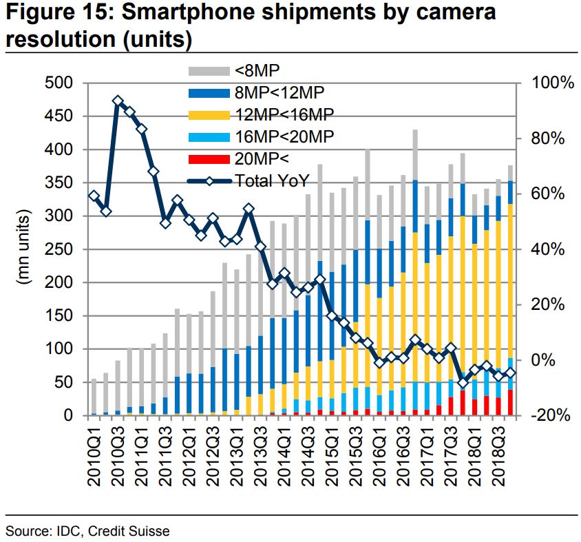
The smartphone market size in terms of units has started to shrink from the end of 2017, according to Credit Suisse:
Velodyne Cumulative Sales Reached $500M
Forbes: Velodyne has shipped 30,000 LiDARs since 2007 when it started making them, generating cumulative sales of $500M, according to the company CEO and founder David Hall.
Velodyne sees demand for shorter-range units for ADAS safety tech, monitoring road conditions, blind spots and objects in a driver's path. “The market is changing a little bit, and we're trying to aim a little bit toward the ADAS end now, where we have lower product costs and higher volume,” David Hall said. “We’re not convinced that the ultimate lidar has been invented by anybody yet. We still have an active program to try to hammer this thing into its final shape.”
Velodyne has formed strategic alliances with three key investors in the past few years, with Ford, China’s Baidu and Nikon investing a combined $200M in the company.
The company built an automated 200,000-square-foot LiDAR “megafactory” in San Jose, CA, in 2017. Nikon is also setting up a LiDAR assembly line in Japan in partnership with Velodyne, and it has a strategic licensing deal with Veoneer, a unit of Swedish Autoliv, to help boost production of its sensors to millions of units a year worldwide.

Saturday, March 23, 2019
Yole on Smartphone Front Camera Market
Yole Developpement publishes its analysis of MWC 2019 smartphone camera announcements "Is the smartphone full display trend taking over from front selfie cameras and biometric 3D sensing?"
"There are obviously two main trends conflicting right now: one favors sensing on the front display side of smartphones; the other favors display.
The display strategy is driven by a ‘wow effect’, by increasing screen-to-body ratio, showing immersive videos that are one of the drivers of 5G adoption. The foldable trend is also an extension of this, and may end up in a compromise between a smartphone and a tablet. It is not clear right now if this could convert into additional revenues or volume for the industry, knowing what we know about smartphones and tablets.
The sensing strategy is using 3D as a biometric interface, where biometry and Human Machine Interface (HMI) are combined. This one conflicts with the full display aesthetic and is constrained by handset design and camera and display technologies. Apple is actively working on the ideal technical solution, which should reach the market before the year’s end."


Friday, March 22, 2019
Color Photon Counting Sensor
Arxiv.org paper "Megapixel Photon-Counting Color Imaging using Quanta Image Sensor" by Abhiram Gnanasambandam, Omar Elgendy, Jiaju Ma, and Stanley H. Chan from Purdue University and Gigajot presents first color photon counting sensor:
"Quanta Image Sensor (QIS) is a single-photon detector designed for extremely low light imaging conditions. Majority of the existing QIS prototypes are monochrome based on single-photon avalanche diodes (SPAD). Color imaging has not been demonstrated with single-photon detectors due to the intrinsic difficulty of shrinking the pixel size and increasing the spatial resolution while maintaining acceptable intra-pixel cross-talk. In this paper, we present image reconstruction of the first color QIS with a resolution of 1024×1024 pixels, supporting both single-bit and multi-bit photon counting capability. Our color image reconstruction is enabled by a customized joint demosaicing-denoising algorithm, leveraging truncated Poisson statistics and variance stabilizing transforms. Experimental results of the new sensor and algorithm demonstrate superior color imaging performance for very low-light conditions with a mean exposure of as low as a few photons per pixel."


"Quanta Image Sensor (QIS) is a single-photon detector designed for extremely low light imaging conditions. Majority of the existing QIS prototypes are monochrome based on single-photon avalanche diodes (SPAD). Color imaging has not been demonstrated with single-photon detectors due to the intrinsic difficulty of shrinking the pixel size and increasing the spatial resolution while maintaining acceptable intra-pixel cross-talk. In this paper, we present image reconstruction of the first color QIS with a resolution of 1024×1024 pixels, supporting both single-bit and multi-bit photon counting capability. Our color image reconstruction is enabled by a customized joint demosaicing-denoising algorithm, leveraging truncated Poisson statistics and variance stabilizing transforms. Experimental results of the new sensor and algorithm demonstrate superior color imaging performance for very low-light conditions with a mean exposure of as low as a few photons per pixel."


Subscribe to:
Posts (Atom)