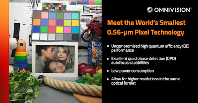
With a pixel size now smaller than the wavelength of red light, OMNIVISION’s R&D team has validated that pixel shrink is no longer limited by the wavelength of light. The 0.56µm pixel design is enabled by a CIS-dedicated 28nm process node and 22nm logic process node at TSMC, with a new pixel transistor layout and 2x4 shared pixel architecture. The pixel is based on OMNIVISION’s PureCel Plus-S stacking technology, and deep photodiode technology is applied to embed the photodiode deeper into the silicon.
“It takes great R&D innovation to advance pixel technology, especially at this level where we are going beyond the wavelength of light,” said Lindsay Grant, SVP of Process Engineering at OMNIVISION. “We have not compromised high performance with the smaller die size. In fact, we have demonstrated comparable QPD and QE performance to our 0.61µm pixel in the visible light range.”
Grant adds, “OMNIVISION invests heavily in R&D and almost 50 percent of our employees comprise R&D engineers. As a global fabless semiconductor provider, we also work closely with our foundry partners, such as TSMC, to develop new process technology approaches that enable industry-leading innovation like this. This is a remarkable achievement, and I applaud our talented R&D team and our foundry partner for their ability to continuously lead the pixel shrink race.”
“We are pleased with the results of our deep collaboration with OMNIVISION in delivery of the world’s smallest 0.56-µm pixel using our industry-leading CIS technology,” said Sajiv Dalal, EVP of Business Management, TSMC North America. “TSMC strives to advance semiconductor manufacturing technologies and services to enable the most advanced, state-of-the-art CIS designs. We look forward to our continued partnership with OMNIVISION to help them achieve high performance, superior resolution, and low power consumption goals and accelerate innovation for their differentiated products.”
The first 0.56µm pixel die will be implemented in 200MP image sensors for smartphones in Q2 2022, with samples targeted for Q3. Consumers can expect to see new smartphones that contain the world’s smallest pixel available on the market in early 2023.

Impressive work! Congrats to the PI & TCAD engineers!
ReplyDeleteBtw, the ikea lighthouse has a misplaced element (ask your kids) ;-)
Haha, the IKEA lighthouse toy is not very popular in China ...
Delete...what is the use of such small pixel?
ReplyDeleteWhat is the value of 200Mp ? Is this a only marketing story and then user shoot 50Mp images 99% of the time?
Sensitivity is 1/4 vs a 1um pixel, and sensitivity matters more than QE
Congratulations to the OmniVision and TSMC teams!
ReplyDeleteIt appears that OV wants to beat Samsung's 0.56um pixel ISSCC paper by a few days!
ReplyDeleteThe ISSCC 2022 Advance Program (referencing Samsung's paper) was published on 02/11/2022, so you could argue Samsung was actually first.
DeleteActually, ISSCC Program was published even earlier:
Deletehttps://image-sensors-world.blogspot.com/2021/12/image-sensors-at-isscc-2022.html
One may even argue that the ISSCC submission deadline was in Sep 2021 so Samsung's work was done even earlier.
DeleteWhat an idiocracy! What about difraction limit? As the man noticed above, all this is nothing but marketing megapixel race, which has nothing to do with image quality progress. We can keep talking about wave lengh and difraction limits, but I am sure, at least, of one thing: human's insanity has no limits!
ReplyDeleteCongratulations to TSMC and the OVT teams, some of the people that commented above are missing the point. This is a great platform to qualify the 28nm CIS on 22nm process that will open the door for other product lines for OVT and future customers of TSMC. This is a strategic program for both companies and a great achievement from a technical perspective. As engineers or marketers we should all give Kudos to the teams involved.
ReplyDeleteGoing to 200MP actually enables end user to use both 2x & 4x in-sensor zoom with decent 12MP resolution.
ReplyDelete