Transforming Infrared Imaging with Emberion’s Cutting-Edge Sensors
Galaxycore: What Is LOFIC? The HDR Technology Behind Advanced Image Sensors
Galaxycore: What Is LOFIC? The HDR Technology Behind Advanced Image Sensors
Link: https://www.prophesee.ai/2026/06/15/prophesee-launches-mantara-event-based-drone-detection/
Prophesee raises €20 million and launches Mantara, the first fully integrated drone detection system built on event-based vision and AI
PARIS, June 15, 2026 – As Eurosatory and Vivatech open their doors this week in Paris, Prophesee – inventor and world leader in event-based perception – announces the launch of Mantara®: the first integrated system built natively event-based for drone detection and tracking. Mantara runs on Hearth®, a new software platform with built-in AI processing.
Field-validated in June 2026, Mantara is powered by Hearth, the platform succeeding OpenEB and the Metavision SDK. These announcements coincide with a €20 million capital raise led by French fund Critical Path Ventures, with participation from existing shareholders. Prophesee is now held by a substantial majority of French shareholders.
Mantara is a camera whose performance rests on integrated sensors that do not capture images but motion and events. Each pixel responds independently, in microseconds, the instant movement occurs. Fast, erratic targets that blur or vanish between frames on a conventional camera remain perfectly visible and fully characterizable by Mantara: in low light, in backlit conditions, against cluttered backgrounds. Low latency is the heart of its edge: in the time a conventional system takes to capture, transfer, and process a single frame, Mantara has already detected a drone, characterized it, and triggered a response or initiated tracking.
This capability is rooted in a bio-mimetic design inspired by the human visual system. The eye does not record the world in full. Instead, it captures sparse, essential signals, and the brain reconstructs and interprets what matters. If Mantara is the eye, Hearth is the brain.
Hearth is built with cybersecurity requirements, GDPR compliance, and AI governance standards baked in. It enables sensor fusion and will ensure backward compatibility across successive generations of Prophesee sensors. Applications built on Metavision and OpenEB will migrate to Hearth seamlessly.
Recent conflicts have put drones at the center of modern warfare, and the threat is moving fast beyond the battlefield: airports, power plants, critical infrastructure, public gatherings. Drones fly low, change direction sharply, and increasingly carry a near-zero signature: minimal electromagnetic emissions, little acoustic output, little thermal trace. They arrive faster, and in greater numbers, with coordinated swarms capable of overwhelming defenses built to track a single target.
Mantara emits nothing. It cannot be detected or jammed. And it learns: Hearth delivers regular updates that allow every deployed unit to adapt to shifts in threat behavior. Ukraine has made this clear: tactics evolve far faster than traditional development cycles can follow.
Civil and Military Missions
Mantara serves both civil and defense use cases. Airports, stadiums, energy and industrial sites, prisons, and ports can integrate it into existing security infrastructure for continuous, automated airspace monitoring. Governments and defense organizations have access to the same system for force protection and counter-UAS operations.
For civil operators, Mantara also offers a compelling privacy advantage: because the sensors detect motion events rather than recording images, Mantara can track moving objects without ever producing footage that could identify individuals. This is a decisive asset for deployment over public spaces and for GDPR compliance.
Hearth: the Reference Platform for the Event-based Ecosystem
Mantara is part of a broader strategic shift encompassing Prophesee’s entire product line.
Hearth will give the event-based ecosystem a trusted reference environment for building scalable, production-grade modules and applications. It will manage sensor updates, backward compatibility, and unlock capabilities that were previously out of reach for developers and integrators working with Prophesee’s patented technology.
As part of this transition, Prophesee announces the end of life of OpenEB, its open-source framework, and of the standalone Metavision SDK. Hearth is the path forward for the developer community. Prophesee will support the migration.
Prophesee’s partners and customers have built a wide range of applications – from eye trackers and ADAS (Advanced Driver Assistance Systems) to ultra-fast cameras for smartphones, ping-pong playing robots, industrial inspection systems, and drone and satellite tracking and targeting solutions. Event-based vision is reaching an inflection point. The market is maturing rapidly and demanding solutions that are robust, secure, and production-ready. With around a hundred patents and multiple sensors to its name, Prophesee has industrialized event-based technology and now intends to structure the broader application ecosystem by making Hearth widely available.
Built with a Network of European Industrial Partners
Mantara benefits from Prophesee’s partnership with IDS Imaging Development Systems GmbH, a leading industrial camera manufacturer. Building on the commercial success of the IDS uEye EVS camera line – based on Prophesee sensors – the two companies expanded their partnership in March 2026 with an agreement signed at Embedded World in Nuremberg to co-develop next-generation industrial vision systems.
Prophesee and Exosens have entered an MoU, paving the way for a long-term partnership to extend bio-mimetic technology beyond the visible spectrum, combining Prophesee’s event-based vision with Exosens’ detection and imaging technologies.
A €20 Million Raise to Anchor Prophesee in France
Prophesee announces a €20 million capital raise led by Critical Path Ventures, a new investor. The team has been reinforced with talent from Google, Microsoft, BCG, Thales, and companies working in drone, robotics, and quantum technologies, as well as from the armed forces. The funds will support the commercial scale-up of Mantara, the development of embedded intelligence within sensors, and the launch of Hearth.
"Ultraviolet Photon Detection in CMOS Single-Photon Avalanche Diodes: A Review" by Wang et al. in IEEE Sensors Journal (vol 26 no 12 June 2026)
DOI: 10.1109/JSEN.2026.3690120
Abstract
Ultraviolet (UV) imaging is enabling a growing range of applications in industrial inspection, biomedicine, and aerospace. Single-photon avalanche diodes (SPADs), known for their exceptional sensitivity and fast timing resolution, have achieved remarkable success in visible and near-infrared (NIR) applications, e.g., in light detection and ranging (LiDAR). However, there remains a significant gap
in the development and deployment of UV SPAD detectors. This review presents the latest progress, challenges, and application potential of SPAD technologies in deep-UV (DUV) and near-UV (NUV) ranges. It reviews the challenges in UV detection and the currently reported NUV SPADs, including wide bandgap semiconductors (WBSs), avalanche photodiodes (APDs), silicon-based SPADs with front-side illumination (FSI) and back-side illumination (BSI), and silicon photomultipliers (SiPMs). By linking UV
imaging with single-photon detection, this review aims to support future silicon-based complementary metal-oxide-semiconductor (CMOS) high-speed, large-format UV SPAD arrays, and their integration into next-generation imaging systems.


Press release (April 2026): https://www.hesaitech.com/hesai-unveils-picasso-6d-full-color-spad-soc-next-gen-etx-and-innovations-in-spatial-intelligence-and-physical-ai/
Hesai Unveils Picasso 6D Full-Color SPAD-SoC, Next-Gen ETX, and Innovations in Spatial Intelligence and Physical AI
Hesai Technology (Nasdaq: HSAI; HKEX: 2525), a global leader in intelligent technology and 3D perception, hosted its 2026 Technology Open Day on April 17, showcasing its latest generation of lidar technologies spanning full-color perception, ultra-high-resolution imaging, and spatial intelligence applications.
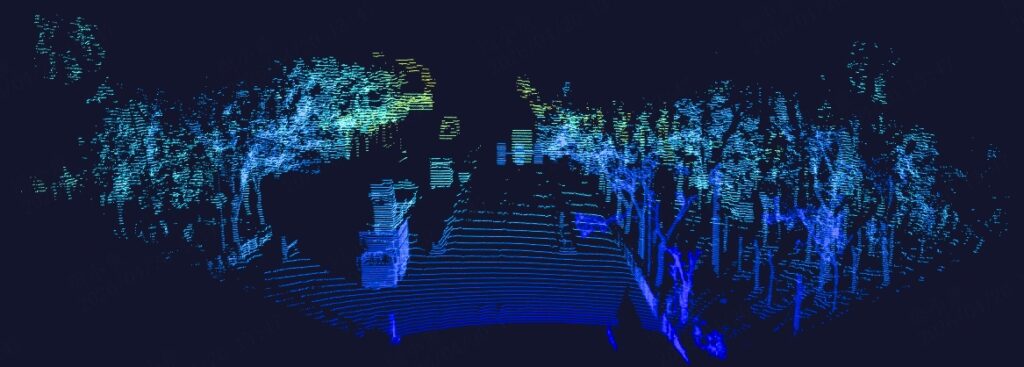
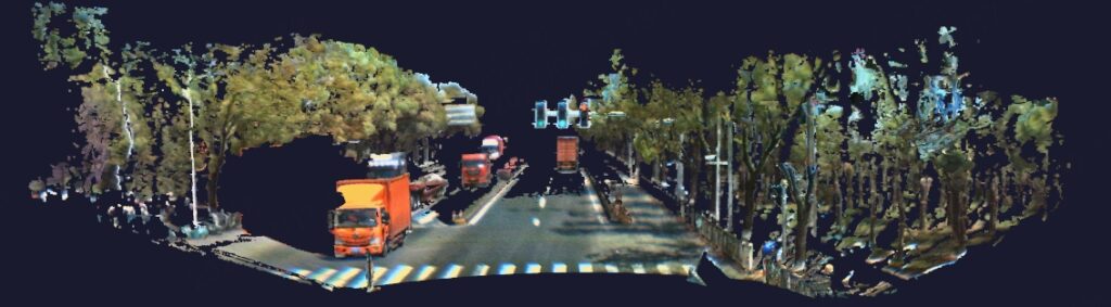
A key highlight was Picasso, the world’s first 6D full-color ultra-sensitive lidar SPAD-SoC, enabling native fusion of spatial and color perception at the ASIC level. Built on this platform, Hesai’s ETX lidar series has been upgraded to support up to 4320 channels and is expected to enter mass production in the second half of 2026. The company also previewed Kosmo, a new spatial intelligence AI hardware product, and outlined a new direction in robotic actuation modules for physical AI systems.
At the core of today’s announcement is Picasso, Hesai’s fifth-generation 6D full-color ultra-sensitive lidar ASIC platform, designed to enable vehicles to see both geometry and color natively on a single chip.
Unlike conventional lidar systems that capture only geometric information such as XYZ, Picasso integrates RGB sensing and time-of-flight (ToF) ranging at the chip-level, enabling the direct generation of colorized point clouds without the need for complex sensor fusion. This 6D full-color capability delivers precise spatial and temporal alignment, resulting in richer environmental understanding and significantly enhancing the perception capabilities of next-generation autonomous systems.
With photon detection efficiency (PDE) exceeding 40%, Picasso delivers industry-leading sensitivity, enabling stronger long-range performance, better detection of small objects, and improved performance in low-light environments within the same power envelope.
Rather than simply combining camera imagery with lidar point clouds, Picasso enables true ASIC-level fusion, with each point inherently carrying color information. This allows autonomous systems to move from spatial perception to real-time understanding of the driving environment, improving performance in different scenarios such as traffic signals, lane markings, and construction zones.
The introduction of Picasso marks a major step in lidar development, moving beyond incremental improvements in resolution toward a new generation of full-color perception. This breakthrough is supported by Hesai’s long-term vertical integration strategy and in-house development across core lidar technologies. Following the launch of Fermi C500, a RISC-V-based high-performance lidar controller SoC that integrates MCU, FPGA functions, and ADC into a single chip, the company has established full-stack in-house ASIC development capabilities. This technology foundation has already translated into large-scale commercialization, with Hesai’s upgraded ATX lidar achieving full-scale mass production and securing over 6 million units in orders from leading OEMs.
Link: https://www.sony-semicon.com/en/news/2026/2026050801.html
Sony Semiconductor Solutions and TSMC Enter Preliminary Agreement for Next-Generation Image Sensor Strategic Partnership
Atsugi, Japan — Sony Semiconductor Solutions Corporation (“Sony”) and Taiwan Semiconductor Manufacturing Company Limited (“TSMC”) (TWSE: 2330, NYSE: TSM) today announced the signing of a non-binding memorandum of understanding (“MOU”) to form a strategic partnership for the development and manufacturing of next-generation image sensors.
Under the proposed partnership, Sony and TSMC intend to establish a joint venture (“JV”), with Sony being the majority and controlling shareholder,to set up development and production lines in Sony’s newly constructed fab in Koshi City, Kumamoto Prefecture. Through the JV, both companies expect to leverage Sony's expertise in sensor design alongside TSMC’s strengths in process technology and manufacturing excellence as part of a broader collaboration aimed at enhancing image sensor performance.
With the MOU signed, Sony and TSMC are discussing potential investments by the JV. These investments, along with new capital investment by Sony in its existing plant in Nagasaki, are being considered on the premise that they would be implemented in phases based on market demand, and that they would receive support from the Japanese government.
This partnership also seeks to explore and address emerging opportunities in physical AI applications, such as automotive and robotics, paving the way for future innovations and expanded technological advancements. The establishment of the JV remains subject to the execution of a definitive legally binding agreement regarding the partnership and the satisfaction of customary closing conditions.
“Building on the trust cultivated through our long-standing collaboration with TSMC, I am delighted that we have reached an agreement to advance our partnership to a new stage,” said Shinji Sashida, President and CEO of Sony Semiconductor Solutions Corporation.“This JV is a significant initiative that brings together the strengths of both companies and aims to drive further advancement in technology and business within the next-generation image sensor field. Building on this JV, Sony intends to further strengthen its business operations with a focus on creating high added value. Rooted in the Sony Spirit that has guided us since our founding, we intend to continue to take on the challenge of creating new markets through unprecedented ideas and distinctive technologies.”
“Sony has been our long-time partner in the CMOS image sensor business. We are excited to elevate our collaboration to the next level, which represents a key step forward in driving future sensing technology in the AI era,” said TSMC Senior Vice President and Deputy Co-COO, Dr. Kevin Zhang. “This partnership underscores our shared commitment and mutual vision of leveraging cutting-edge technologies and innovative solutions to deliver leading sensing technology and products. We look forward to working closely together to achieve impactful results and create lasting value for all stakeholders.”
Image Sensors Blog is soliciting 1-2 volunteers to help me maintain our weekly posting schedule. We have a large readership spanning industry and academia. This is a great opportunity esp. for an early-career academic (graduate student/postdoc) to provide valuable service to the image sensors community. Please email me (see contact listed in the "Blog Authors" sidebar) with a short introduction and how you see yourself contributing to the blog.
Many thanks to Dave Gilblom who is now retiring from his role as one of the blog maintainers. Thanks, Dave, for the countless hours of hard work poring over image sensor documentation, and for spearheading the Job Postings and Conference List features on the blog!
Advanced Packaging and Multi-Dimensional Systems Integration for Image Sensors
November 5 & 6, 2026
Antwerp, Belgium
Abstract
Packaging technology for image sensors is an underappreciated issue in the systems integration process, greatly affecting performance, scalability, physical area, and cost. The multi-dimensional package as well as the underlying technology can greatly affect the overall electrical, optical, mechanical, and thermal characteristics of the integrated system. These systems have become multi-dimensional in nature, composed of several interacting layers and multiple sensors with the imagers vertically integrated within the overall system. Now that image sensors are driven more than ever to extreme performance capabilities, novel packaging options and technologies have become increasingly important. An important trend to support large scale sensors integrated into systems are the widely applied stacking and chiplet technologies in which several layers of active silicon are placed above each other. In this way, highly compact, high performance imaging systems are becoming possible. Packaging of systems including image sensors has become much more than placing a single silicon die into a package and attaching some wires.
The landscape of image sensor applications is widening at an accelerating rate, requiring new and different packaging solutions. This forum will review this key issue as well as include a series of highly related topics. This year’s Harvest Imaging Forum is focusing on the existing field of multi-dimensional packaging technology for image sensors. Related topics such as on-chip interconnect, power delivery, synchronization, network communication, thermal behavior, and heterogeneous integration will also be discussed. The focus will be on both current and near term capabilities. These next generation technologies are now becoming available, allowing the development and integration of large scale systems composed of multiple layers and chiplets to produce large scale systems operating at increasingly higher levels of performance.
[ST Press Release from April 2026.]
STMicroelectronics brings always-on vision to next-generation personal electronics with new ultralow-power image sensors
VD55G4 and VD65G4 extend the ST BrightSense portfolio with compact, ultralow-power, microcontroller-compatible sensors for wearables, AR/VR, and smart devices
These new global-shutter image sensors can consume up to 10x less, in operating mode at around 800×700 resolution and 10 frames per second
Geneva, Switzerland — April 28, 2026 — STMicroelectronics (NYSE: STM), a global semiconductor leader serving customers across the spectrum of electronics applications, introduces a new generation of ultralow-power global-shutter image sensors that deliver high-quality, always-on vision to compact devices operating on batteries or harvested energy. The VD55G4 (monochrome) and VD65G4 (RGB color) sensors, part of the ST BrightSense portfolio, are now available to early adopters, enabling customers to start designing their next generation of smart, ultralow-power vision devices today.
Designed for the next wave of personal electronics and smart devices, the new sensors serve applications including wearables, AR/VR and XR headsets, smart home appliances and medical devices. They are engineered to deliver rich visual context and AI-ready data under tight constraints on power, size, and cost. The sensors combine an ultralow-power detect-and-wake architecture with a very small global-shutter optical format and interfaces optimized for low-power microcontrollers and cost-effective systems on chips (SoCs).
“Always‑on vision is becoming essential for the next generation of personal electronics, from smart glasses and AR/VR headsets to intelligent home appliances and medical devices. With VD55G4 and VD65G4, we are bringing this capability to smaller, lighter products that must run for a long time on a tiny battery. These new sensors help our customers create more intuitive and responsive experiences, extend battery life, and bring embedded vision and edge AI into everyday devices,” said Alexandre Balmefrezol, Executive Vice President and General Manager of the Imaging Sub-Group at STMicroelectronics.
From wearables and AR/VR to smart appliances
VD55G4 and VD65G4 bring always‑on vision to products that must stay small, light, and extremely power‑efficient. Building on the ST BrightSense family, they add a color option, faster response for interactive use cases, and simple connectivity to low‑power microcontrollers, making it easier to add vision to space‑ and cost‑constrained designs.
In wearables, the sensors enable all‑day, always‑aware features such as glance detection, presence sensing, and contextual alerts, while fitting into very compact designs and working directly with microcontroller‑based platforms.
For AR/VR and XR headsets, they combine low power and high‑quality capture to support accurate tracking and spatial awareness, helping extend battery life without compromising comfort.
In smart home appliances, IoT devices, and medical products, the sensors allow more intelligence to run locally on the device itself, reducing cloud dependence and standby power. Their tiny size and energy efficiency also make them well suited to solar‑ or energy‑harvesting‑powered vision nodes.
Ultralow‑power design that consumes up to 10x less
Thanks to an optimized sensor architecture and dedicated always‑on mode, VD55G4 and VD65G4 can consume up to 10 times less power than conventional global‑shutter sensors. They can watch for changes in a scene and wake up the main processor only when needed, shifting from continuous streaming to event‑driven operation. This enables all‑day, always‑on experiences, longer battery life, and practical vision systems powered by small batteries or energy harvesting.
Their very small footprint and integrated image processing simplify design and reduce system cost, while supporting responsive, AI‑ready vision features in a wide range of edge devices.
Link: https://it.chosun.com/news/articleView.html?idxno=2023092160385
"Lee Je-seok, Vice President and Chief Technology Officer (CTO) of the Sensor Business Team, also resigned recently after 32 years at the company. Lee is considered a "living witness" of Samsung’s image sensor brand, ISOCELL, and is credited with leading the development of the world's first 100-megapixel and 200-megapixel sensors, as well as securing a spot in Apple’s supply chain.
Following his resignation, Lee is reportedly preparing to launch an image sensor startup. On social media, he posted an image signaling a "stealth mode" startup with global experts, stating he would "redefine the future of imaging in January 2027." Industry observers are closely watching as a key designer of Samsung's proprietary technology could emerge as a potential competitor."
18th International Conference on Sensing Technology (ICST2026) - 7-9 December 2026 - Sydney, Australia - Website
International Technical Exhibition on Image Technology and Equipment (ITE) - 2-4 December 2026 - Yokohama, Japan - Website
IEEE International Electron Devices Meeting - 12-16 December 2026 - San Francisco, CA, USA - Website
If you know about additional local conferences, please add them as comments.
Return to Conference List index
Press release: https://www.usa.canon.com/newsroom/2026/20260415-camera
Canon U.S.A. Sets New Standard in Low-Light Imaging with the Launch of the MS-510 Multi-Purpose Camera at NAB 2026
Featuring a new Canon 1-inch SPAD sensor, the MS-510 delivers impressive low-light and long-range performance for ultra-low-light environments
MELVILLE, N.Y., April 15, 2026 – Canon U.S.A., Inc., a leader in digital imaging solutions, today announced the release of the MS-510, an innovative multi-purpose camera engineered to meet the rigorous demands of ultra-low-light full-color video shooting. Building on the success of the MS-500, the new MS-510 is designed to deliver high-fidelity captures of everything from nocturnal wildlife and natural nightscapes to high-security areas such as seaports, public infrastructure facilities, and national borders where "seeing the unseen" is a mission-critical requirement.
In response to increasing demands for excellent performance in near-total darkness, the MS-510 features a new Canon 1-inch Single-Photon Avalanche Diode (SPAD) sensor with the world’s highest number of pixels at approximately 3.2 million with improved Near-Infrared (NIR) sensitivity.
By leveraging this technology, the camera achieves a minimum subject illumination of 0.0006 lux, a significant improvement over the 0.001 lux of its predecessor. This allows for bright, full-color imaging in ultra-low-light environments where traditional cameras can fail. Furthermore, the MS-510 boasts improved NIR capabilities, providing a tactical advantage for night-mode operations and long-distance detection.
The MS-510 is not just a camera; it is a sophisticated tool for critical infrastructure monitoring and law enforcement. Key features include:
Designed to fit into existing security ecosystems, the MS-510 shares common protocols with the MS-500, including NU, Pelco-D®, ONVIF®, and WebView. It offers versatile output options, including 3G/HD-SDI for high-quality video feeds and a LAN terminal for IP-based camera control and distribution.
Why Samsung Can't Beat Sony's Image Sensors:
China’s Newest Tech Billionaire Made His Fortune From Developing Image Sensor Chips For Robotics:
Jinwen Wei and Liangcai Cao, "Compact Neural Pancake Camera for High-Perceptual-Quality Foveated Imaging," ACS Photonics (2026).
Link: https://doi.org/10.1021/acsphotonics.6c00691
Pancake catadioptric optics utilize optical folding to effectively reduce the optical-path thickness in virtual-reality display systems. However, limited optical throughput and optical degradation make image reconstruction for pancake cameras severely ill-posed, hindering broader imaging applications. In this article, we propose a neural pancake camera with adaptive-prior deconvolution, achieving compact, high-perceptual-quality imaging. By introducing latent-space projection, adaptive prior deconvolution alleviates the trade-off between pixel fidelity and perceptual quality and addresses the excessive smoothing inherent in conventional pixelwise optimization. The proposed neural pancake camera reduces the ratio of axial length to physical aperture diameter by 3.2 times compared with other flat cameras with high imaging quality. Experiments and ablation studies substantiate that the proposed adaptive prior deconvolution improves perceptual quality by 70%, as measured by CLIP-IQA, while also outperforming the state-of-the-art deep learning models on pixel-level fidelity. As a representative application of the proposed neural Pancake camera, this work further showcases bioinspired foveated imaging, highlighting its potential for bandwidth-efficient imaging in next-generation edge and portable devices.

Figure 1. Pipeline of the proposed neural Pancake camera. (a) Conceptual illustration of the proposed compact Pancake camera scheme. (b) The inherent trade-off between perceptual quality and pixel-level quality of computational imaging. This work proposes adaptive prior deconvolution to promote the perceptual imaging quality of Pancake cameras while improving pixel fidelity. (c) Overview of the training process of the end-to-end adaptive prior deconvolution. The framework operates by optimizing the learnable deconvolution network while leveraging a latent natural-image manifold prior, anchoring the restoration output to the natural image manifold to reconcile the perceptual-pixel trade-off.

Figure 3. Quantitative evaluation and visualization of the adaptive-prior deconvolution. (a) Schematic illustration of the inference process based on the adaptive-manifold prior. (b) Quantitative performance profiles of averaged MUSIQ, SSIM, and PP-IQA across inference steps. (c) Visual comparisons demonstrating the effects of the low prior, the adaptively selected proper prior, and the over-prior.

Figure 4. Demonstration of neural Pancake camera-based foveated imaging. (a) Schematic illustration of foveated imaging in the human visual system. (b) Profiles of high-frequency content proportion and relative acuity versus field of view. (c) Comparison of reconstructed and raw-captured images across different fields of view.
Link: https://imagesensors.org/CFP2027/fcfp2027.pdf
FIRST CALL FOR PAPERS ABSTRACTS DUE Dec 10, 2026
2027 International Image Sensor Workshop
The Westin Resort & Spa, Whistler, BC, Canada
June 13-17, 2027
The 2027 International Image Sensor Workshop (IISW) provides a biennial opportunity to present innovative work in the area of solid-state image sensors and share new results with the image sensor community. The event is intended for image sensor technologists; in order to encourage attendee interaction and a shared experience, attendance is limited, with strong acceptance preference given to workshop presenters. As is its tradition, the 2027 workshop will emphasize an open exchange of information among participants in an informal, secluded setting besides Whistler, BC, Canada.
The scope of the workshop includes all aspects of electronic image sensor design and development. In addition to regular oral and flash presentation papers, the workshop will include invited talks and announcement of International Image Sensors Society (IISS) Award winners.
Image Sensor Design and Performance
CMOS imagers, CCD imagers, SPAD sensors
New and disruptive architectures
Global shutter image sensors
Low noise readout circuitry, ADC designs
Single photon sensitivity sensors
High frame rate image sensors
High dynamic range sensors
Low voltage and low power imagers
High image quality; Low noise; High sensitivity
Improved color reproduction
Non-standard color patterns with special digital processing
Imaging system-on-a-chip, On-chip image processing
Event-based image sensors
Pixels and Image Sensor Device Physics
New devices and pixel structures
Advanced materials
Ultra miniaturized pixels development, testing, and characterization
New device physics and phenomena
Electron multiplication pixels
Techniques for increasing QE, well capacity, reducing
crosstalk, and improving angular response
Front side illuminated, back side illuminated, and
stacked pixels and pixel arrays
Pixel simulation: Optical and electrical simulation, 2D and
3D, CAD for design and simulation, improved models
Application Specific Imagers
Image sensors and pixels for range sensing: TOF, RGBZ,
Structured light, Stereo imaging, etc.
Image sensors with enhanced spectral sensitivity (NIR, UV, IR)
Sensors for DSC, DSLR, mobile, digital video cameras and mirror-less cameras
Array imagers and sensors for multi-aperture imaging, computational imaging, and machine learning
Sensors for medical applications, microbiology, genome sequencing
High energy photon and particle sensors (X-ray, radiation)
Line arrays, TDI, Very large format imagers
Multi and hyperspectral imagers
Polarization sensitive imagers
Image sensor manufacturing and testing
New manufacturing techniques
Wafer-on-wafer and chip-on-wafer stacking technologies
Backside thinning
New characterization methods
Packaging and testing: reliability, yield, cost
Defects, noises, and leakage currents
Radiation damage and radiation hard imagers
On-chip optics
Advanced optical path, color filters, microlens, light guides
Nanotechnologies for Imaging
Wafer level cameras
Submission of abstracts:
An abstract should consist of a single page of maximum 500-words text with up to two pages of
illustrations (3 pages maximum), and include authors’ name(s) and affiliation, mailing address,
telephone and e-mail address.
The deadline for abstract submission is 11:59pm, Thursday Dec 10th, 2026 (PST).
To submit an abstract, please go to: https://cmt3.research.microsoft.com/IISW2027
Above website should be open by Aug 1st, 2026.
The first time you visit the paper submission site, you'll need to click on "Create Account". Once you create and verify your account with your email address, you will be able to submit abstracts by logging in and clicking “Create New Submission”.
Please visit http://imagesensors.org/CFP2027 for complete instructions and any updates to the
abstract and paper submission procedures.
Abstracts will be considered on the basis of originality and quality. High quality papers on work in progress are also welcome. Abstracts will be reviewed confidentially by the Technical Program
Committee.
Key Dates
Authors will be notified of the acceptance of their abstract by February 12th, 2027.
Final-form 4-page paper submission date is March 20th, 2027.
Presentation material submission date is April 30th, 2027.
Location and format:
The IISW 2027 will be held at the Westin Resort & Spa in Whistler, British Columbia in Canada.
Registration, Workshop fee and Program:
The Workshop Program and registration details will be provided in the Final Announcement of the Workshop.
In a paper titled "Design and Optimization of a Twisted Photodiode Pixel Structure for All-Directional Phase-Detection Autofocus CMOS Image Sensors" a team from Canon write:
To achieve an all-directional and high-speed, high-accuracy autofocus (AF) function, we propose a CMOS image sensor with a Twisted Photodiode (PD) structure. The developed 3D-stacked back-side illuminated (BSI) sensor employs the Twisted PD, which enables equivalent angular response characteristics in both the horizontal and vertical directions for the two PDs integrated within a single pixel, thereby realizing AF detection for all pixels and all directions. This paper describes the Twisted PD structure that enables all-directional AF and presents an analysis of charge transfer behavior in this unique 3D configuration. In this paper, “all-directional” refers to robustness with respect to subject direction.
This paper was published in the IISW2025 special issue of Sensors.
Link: https://www.mdpi.com/1424-8220/26/6/1758


Omnivision is listed on HKSE https://www.reuters.com/world/asia-pacific/chinas-omnivision-open-slightly-higher-hong-kong-trading-debut-2026-01-12/
ESA, CNES, AIRBUS DEFENCE & SPACE, ISAE-SUPAERO, OHB, SODERN, and THALES ALENIA SPACE are pleased to invite you to:
VISSA: VISible detection for Space Applications, the 9th iteration of the workshop series known as “Space & Scientific CMOS Image Sensors”
Please find attached the CALL FOR ABSTRACTS for the workshop planned for 24 and 25 November at ESA-ESTEC, The Netherlands.
This is a very popular event and has become one of the main European technical exchanges on CMOS image sensors. The aim of this workshop is to focus on latest developments in advanced image sensors for scientific and space applications targeting wavelengths shorter than 1.1 μm.
The deadline for abstract submission is 4 September 2026.
Please send a short abstract on one A4 page maximum in word or pdf format giving the
title, the author name(s) and affiliation(s), and presenting the subject of your talk, to
matthew.soman@esa.int and valerian.lalucaa@cnes.fr
Abstracts shall preferably address one or more of the following topics:
• Pixel design (high QE, FWC, MTF optimization, low lag, …)
• Electrical design (low noise amplifiers, shutter, CDS, high speed architectures, TDI, HDR, …)
• On-chip ADC or TDC (in pixel, column, …)
• On-chip processing (smart sensors, multiple gains, summation, corrections)
• Low-light detection (electron multiplication, avalanche photodiodes, quanta image sensors, …)
• Photon counting, Time resolving detectors (gated, time-correlated single-photon counting, …)
• Hyperspectral architectures
• Materials (thin film, optical layers, dopant, high-resistivity, amorphous Si, …)
• Processes (backside thinning, hybridization, 3D stacking, anti-reflection coating, …)
• Packaging
• Optical design (micro-lenses, trench isolation, filters, …)
• Large size devices (stitching, butting, …)
• High speed interfaces
• Focal plane architectures
• CMOS image sensors with recent space heritage showing in-flight performance
Workshop format & official language
Oral presentations shall be requested for the workshop. The official workshop language is English.
Slide submission
After abstract acceptance notification, the authors will be requested to prepare their presentation in pdf
or Powerpoint file format, to be presented at the workshop. Authors will also be required to provide a
version to the organizing committee along with an authorization to make it available for Workshop
attendees, and on-line for the COMET members. No proceedings will be compiled and so no detailed
manuscript needs to be submitted.
Registration
Registration fee : Attendees: 120 Euro // students: 60 Euro
On-line registration link will be sent at registration opening.
Exhibition/Sponsorship:
Booths will be available during the workshop. If you are interested to exhibit, please contact the
organizing committee.
Product overview page: https://www.sony-semicon.com/en/products/is/scientific/x-ray.html
The IMX711 is an X-ray image sensor that employs a direct conversion and integration type CMOS technology, in which X-rays and electron beams are detected directly.
It uses proprietary technology to achieve both high-speed capture and low noise performance, enabling the detection of weak single-photon signals, which is difficult with conventional integration type sensors.
This technology enables measurement with a wider dynamic range than conventional methods, offering from single-photon detection under low-flux conditions to stable and high-accuracy measurement in high-flux conditions.
The image sensor can capture energy, spatial, and temporal information simultaneously, which contributes to better measurement accuracy, measurement throughput, and flexible post-processing depending on the application and use casein advanced device inspection and scientific measurements such as materials science and life sciences.


In a June 2026 paper titled "A 400×400 3.24-μm 117-dB Dynamic Range Three-Layer Stacked Digital Pixel Sensor With Triple Quantization and Fixed Pattern Noise Correction" published in IEEE Trans. Electron Devices, a team from Brillnics, Meta, and SesameAI* write:
This article presents a 400×400 digital pixel sensor (DPS) with a 3.24 μm pixel pitch, fabricated using a 45/40/40 nm three-layer stacked process. The sensor achieves single-exposure high dynamic range (SEHDR) through overlapped triple quantization (3Q), fixed pattern noise correction (FPN-C), and black level correction (BLC). An on-chip image signal processor (ISP) is integrated to support defect pixel correction (DPC), SEHDR linearization, and gamma correction. Sparse transmission (ST) is incorporated to reduce transmitted data volume and, consequently, transmission power consumption. A wafer-level chip-scale package (WLCSP) with two redistribution layers (RDLs) is employed, resulting in a compact form factor of 2.47×1.85 mm^2. This work achieves a dynamic range (DR) of 117 dB while consuming 2.45 mW at 30 frames/s (fps), yielding a figure of merit (FoM) of 0.0046 e- rms pJ, and is developed to meet the growing demands of augmented reality (AR) and virtual reality (VR) applications.
Full paper: https://doi.org/10.1109/TED.2026.3687537


* Sesame AI (https://www.sesame.com/) is developing "conversational AI agents", with a smart glasses product slated for 2027.
IEEE Nuclear Science Symposium, Medical Imaging Conference, and Room-Temperature Semiconductor Detectors Symposium - 7-14 November 2026 - Granada, Spain - Website
SPIE Future Sensing Technologies 2026 - 9-12 November 2026 - Yokohama, Japan - Website - (co-located with SPIE Asia-Pacific Remote Sensing and Photonics Innovation)
Sensing with Quantum Light (SQL26) - 9-13 November 2026 - Cologne, Germany - Website
electronica - 10-13 November 2026- Munich Germany - Website
Compamed - 16-19 November 2026 - Dusseldorf, Germany - Website
Sensors 2026 - 19-21 November 2026 - Osaka, Japan - Website
18th Symposium Sensor Data Fusion: Trends, Solutions and Applications - Bonn, Germany - 23-25 November 2026 - Website
9th VISSA: Visible Detection for Space Applications - 24-25 November 2026 - Noordwijk, the Netherlands - Website
RSNA 2026 - 29 November-3 December 2026 - Chicago, Illinois, USA - Website
If you know about additional local conferences, please add them as comments.
Return to Conference List index


Wetzlar, Germany & Changchun, China, 20 April 2026 Today, Leica Camera AG and Gpixel, a leading global provider of advanced CMOS image sensors, announce a strategic partnership. Both partners agreed to combine their core competencies in the area of innovative imaging technologies to
co-develop a new high performance imaging sensor tailored for next-generation Leica cameras. This collaboration brings together Leica’s long-standing expertise in premium imaging and Gpixel’s cutting-edge sensor design capabilities to push the boundaries of what is technically possible in digital photography.
The partnership focuses on jointly engineering a bespoke image sensor optimized for Leica’s rigorous imaging standards, enabling unprecedented levels of image quality, dynamic range, color fidelity, and low-light performance across future Leica products.
Dr. Andreas Kaufmann, Chairman of the Supervisory Board and majority shareholder Leica Camera AG said: „I am really happy and proud that our long-term cooperation with Gpixel will result in a true Leica sensor, incorporating the best ingredients of engineering between Wetzlar, Antwerp and Changchun.”
“At Gpixel, we have always admired Leica’s uncompromising approach to craftsmanship and image performance,” said Xinyang Wang, CEO of Gpixel. “Collaborating with Leica gives us the opportunity to combine our sensor-engineering strengths with their legendary imaging heritage. This partnership allows us to co-create a new generation of sensors that will empower photographers with extraordinary image-making capabilities.”
The jointly developed sensor will be purpose-engineered to meet the highest performance requirements in color reproduction, noise optimization, dynamic range, and detail rendering. The collaboration also includes close cooperation in validation, image tuning, and production readiness.
About Gpixel
Gpixel is a global leader in advanced CMOS image sensor solutions, serving industrial, professional, and scientific imaging markets. Known for delivering state-of-the-art performance across a broad portfolio of sensor technologies—from high-resolution and high-speed imaging to low-noise and specialized sensor architectures—Gpixel helps partners across the world bring next-generation imaging products to life.
About Leica Camera
Leica Camera AG is an international, premium manufacturer of cameras, lenses and sports optics. As part of its growth strategy, the company has expanded its portfolio to include mobile imaging (smartphones) and the manufacture of high-quality spectacle lenses and watches, and is also represented in the home cinema segment with its own projectors.
Leica Camera AG, having its headquarters in Wetzlar, Germany, and a second production site in Vila Nova de Famalicão, Portugal, operates a global network of its own distribution companies with around 120 Leica Stores worldwide.
The Leica brand stands for excellence in quality, German craftsmanship and industrial design, combined with innovative technologies. An integral aspect of the brand culture is the promotion of the culture of photography, with around 30 Leica Galleries worldwide, the Leica Akademie and international awards such as the Leica Hall of Fame Award and the Leica Oskar Barnack Award (LOBA).
VISION - 6-8 October 2026 - Stuttgart, Germany - Website
Photonics Spectra Sensing Technologies Summit 2026 - 7 October 2026 - Online - Website
Optica Laser Congress and Exhibition - 11-15 October 2026 - Vilnius, Lithuania - Website
ASNT Annual Conference - 12-15 October 2026 - Columbus, Ohio, USA - Website
CPAD 2026 (Coordinating Panel for Advanced Detectors) - 20-23 October 2026 - Seattle, Washington, USA - Website
SPIE/COS Photonics Asia - 24-26 October 2026 - Nantong, Jiangsu, China - Website
IEEE Sensors Conference - 25-28 October 2026 - Rotterdam, The Netherlands, - Website
Image Sensors Asia - 28-29 October 2026 - Seoul, South Korea/Hybrid - Website
If you know about additional local conferences, please add them as comments.
Return to Conference List index
Link: https://www.photonics.com/Articles/Single-Photon-Detection-Bridges-the-Gap-Between/p7/a71989
Single-Photon Detection Bridges the Gap Between Quantum Tech and Industrial Users
The article covers the following companies and startups:
AlpsenTek Completes Series B+ as Hybrid Vision Sensors Become a New Gateway to the AI-Powered Physical World
SHENZHEN, China — March 17, 2026 — AlpsenTek, a pioneer in hybrid vision sensor technology, today announced the completion of a Series B+ financing round and the total fund-rasing has surpassed 100 million USD.
The B+ round was jointly backed by BEIDM, Guangdong Finance Fund Management, GAC Capital, Circumference Capital, Changjiang Capital, Bluetrum, UNICC Capital, Zhichen Investment, Wofo Venture Capital, and Sunyes.
The new funding will support continued core technology development, large-scale product manufacturing, and global market expansion, accelerating the industrial adoption of next-generation AI vision sensing technologies.
The Growing Need for Real-Time Perception in Physical AI
As artificial intelligence moves beyond the digital world and increasingly interacts with the physical environment, real-time environmental perception is becoming a fundamental infrastructure for intelligent systems.
Traditional vision sensors, which rely on fixed-frame-rate image capture and full-pixel data acquisition, are gradually struggling to meet the emerging requirements of intelligent perception systems that demand high speed, low latency, and high dynamic range.
Hybrid Vision Sensing: A New Path for AI Machine Vision
AlpsenTek’s Hybrid Vision Sensor (HVS) technology introduces a new technical paradigm for machine vision systems.
The technology integrates frame-based image sensing and event-based sensing mechanisms on a single sensor chip, enabling devices to simultaneously capture both image information and brightness change signals within a scene. This provides AI systems with visual inputs that are both more efficient and more representative of real-world dynamics.
If traditional image sensors record “what the world looks like,” hybrid vision sensors capture both “what the world looks like” and “how the world is changing.”
Dual-Modality Perception for Next-Generation AI
Compared with vision systems that rely solely on frame-based images, hybrid vision sensors can detect scene changes with much higher temporal resolution while maintaining full image output capability.
This dual-modality perception approach allows AI systems to achieve more stable and efficient visual perception in high-speed motion, high dynamic range, and complex lighting environments.
For rapidly developing AI applications—including robotics, autonomous driving, and intelligent devices—machines must not only see two-dimensional image details, spatial structure, and color, but also understand how environments evolve over time.
By introducing the temporal dimension alongside traditional visual information, hybrid vision sensors enable machines to more effectively perceive object motion, interactions, and environmental changes, significantly enhancing a system’s ability to understand the real world.
Reducing Data Redundancy for Efficient Edge AI
At the same time, traditional visual systems generate large amounts of redundant data during video capture, requiring substantial computational resources for processing.
Hybrid vision sensors adopt an event-driven sensing mechanism, outputting key information only when changes occur in a scene. This reduces redundant data generation at the source and provides more efficient data input for edge AI systems.
In the AI era, vision sensors are evolving from simple imaging devices into core interfaces through which machines perceive and understand the physical world.
CEO Perspective
Deng Jian, founder and CEO of AlpsenTek, said the rapid transition of AI from digital environments into the real world is reshaping the role of perception technologies.
“Artificial intelligence is rapidly moving from digital space into the real world,” Deng said. “Future AI systems—whether robots, intelligent devices, or automated systems—will require continuous, real-time perception of the physical environment. Hybrid vision sensors were developed to meet this demand. By simultaneously providing image information and motion-change data, we aim to build a more efficient visual perception foundation for the next generation of intelligent systems.”
Building a Hybrid Vision Product Ecosystem
As a key innovator in hybrid vision technology, AlpsenTek has established a complete proprietary technology stack spanning pixel architecture, chip design, and vision algorithms, and has been among the first globally to achieve large-scale production of hybrid vision sensors.
In 2025, the company introduced the APX014 (ALPIX-Pizol) hybrid vision sensor designed for edge AI perception applications, along with the APX002 (ALPIX-Maloja) pure event-based vision sensor.
Together with the previously released APX003 series and APX004 series, the company has formed a growing product portfolio targeting applications across robotics, wearables, smart home devices, automotive electronics, and consumer electronics.
Accelerating Industry Adoption
AlpsenTek is currently collaborating with several leading global technology companies to advance the large-scale adoption of hybrid vision sensors in intelligent devices and AI systems.
Deng said the company is entering a stage of acceleration as AI vision technologies move toward mass deployment.
“We are now at a pivotal moment for AI vision technologies to move into large-scale applications,” Deng said. “Over the next decade, countless intelligent systems will enter the real world, and visual perception will be one of their most fundamental technologies. Our goal is to make hybrid vision sensors one of the key perception interfaces for next-generation intelligent devices.”
As AI and intelligent hardware continue to evolve, new visual perception technologies are entering an unprecedented phase of opportunity. AlpsenTek said it will continue advancing core technological innovation and product commercialization to expand hybrid vision sensing into more real-world applications.
In an era where AI is moving into the physical world, machines must first learn to see the world—and see its changes—efficiently.