Miyazawa et al. from Shizuoka University in Japan recently published an article titled "A Time-of-Flight Image Sensor Using 8-Tap P-N Junction Demodulator Pixels" in the MDPI Sensors journal.
[Open access: https://www.mdpi.com/1424-8220/23/8/3987]
Abstract:
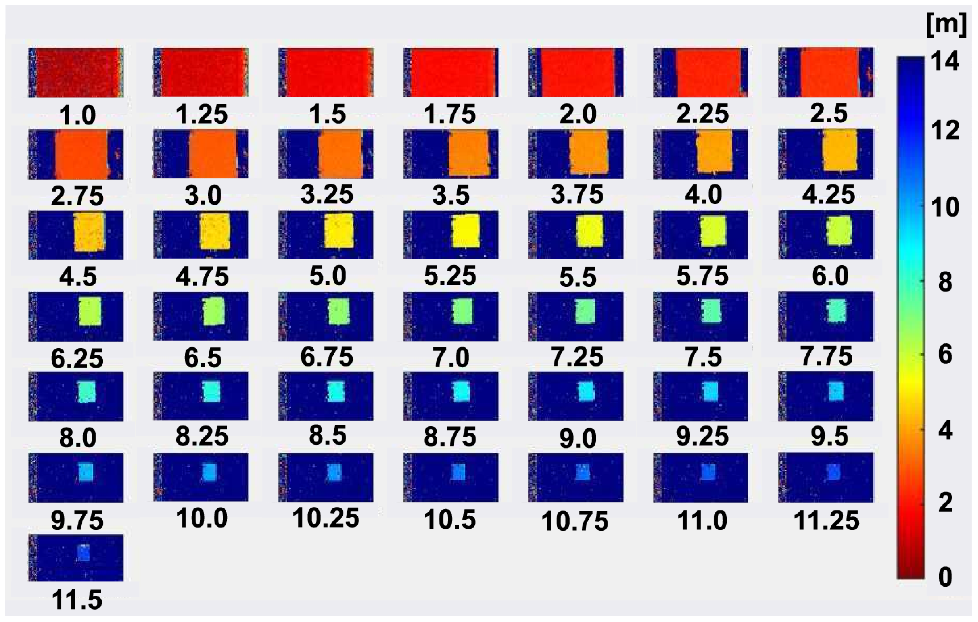
This paper presents a time-of-flight image sensor based on 8-Tap P-N junction demodulator (PND) pixels, which is designed for hybrid-type short-pulse (SP)-based ToF measurements under strong ambient light. The 8-tap demodulator implemented with multiple p-n junctions used for modulating the electric potential to transfer photoelectrons to eight charge-sensing nodes and charge drains has an advantage of high-speed demodulation in large photosensitive areas. The ToF image sensor implemented using 0.11 µm CIS technology, consisting of an 120 (H) × 60 (V) image array of the 8-tap PND pixels, successfully works with eight consecutive time-gating windows with the gating width of 10 ns and demonstrates for the first time that long-range (>10 m) ToF measurements under high ambient light are realized using single-frame signals only, which is essential for motion-artifact-free ToF measurements. This paper also presents an improved depth-adaptive time-gating-number assignment (DATA) technique for extending the depth range while having ambient-light canceling capability and a nonlinearity error correction technique. By applying these techniques to the implemented image sensor chip, hybrid-type single-frame ToF measurements with depth precision of maximally 16.4 cm (1.4% of the maximum range) and the maximum non-linearity error of 0.6% for the full-scale depth range of 1.0–11.5 m and operations under direct-sunlight-level ambient light (80 klux) have been realized. The depth linearity achieved in this work is 2.5 times better than that of the state-of-the-art 4-tap hybrid-type ToF image sensor.
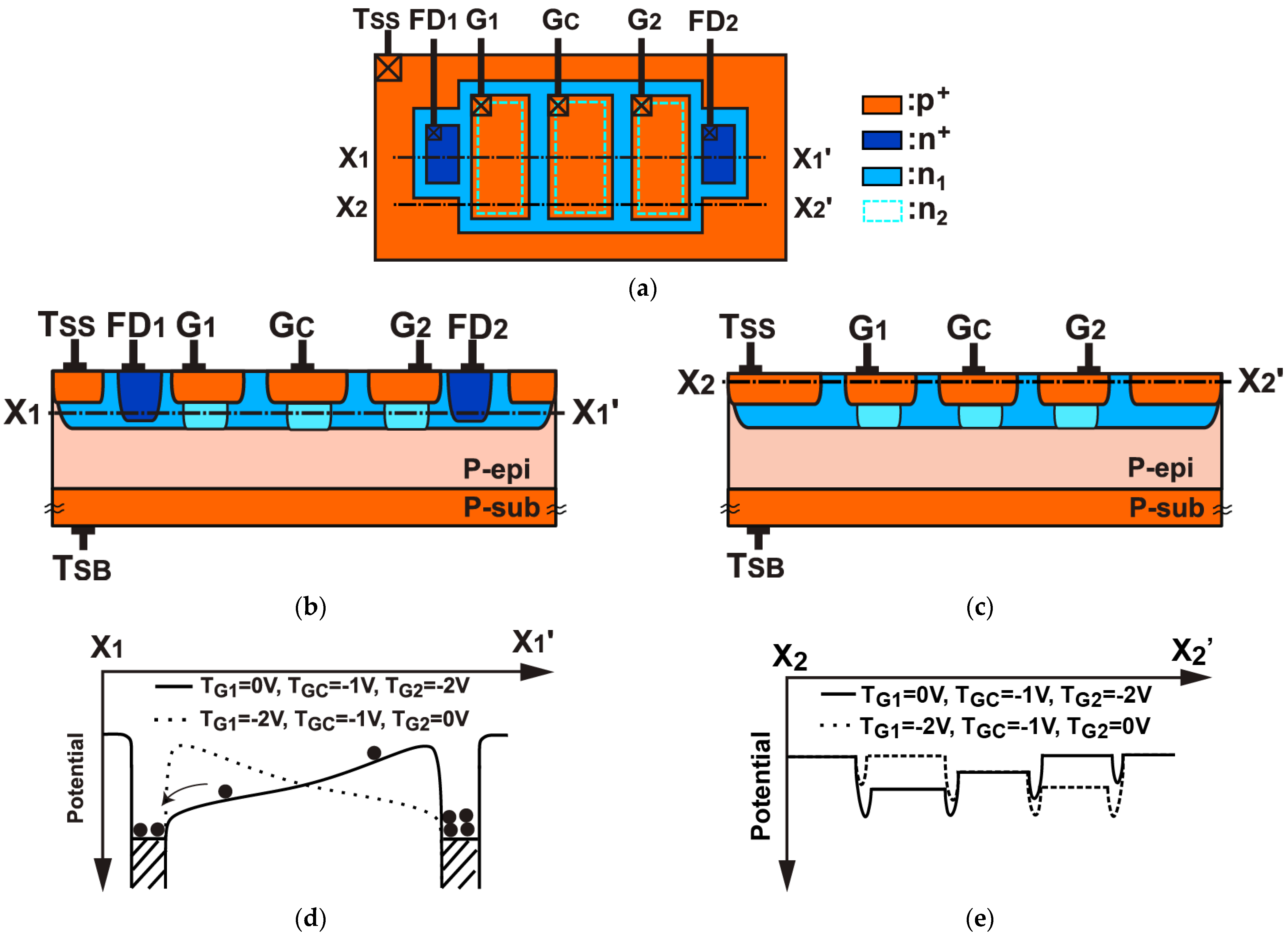
Figure 1. Structure and principle of the two-tap p-n junction demodulator (PND): (a) Top view; (b) Cross-sectional view (X1–X1’); (c) Cross-sectional view (X2–X2’); (d) Potential diagram at the channel (X1–X1’); (e) Potential diagram at Si surface (X2–X2’).
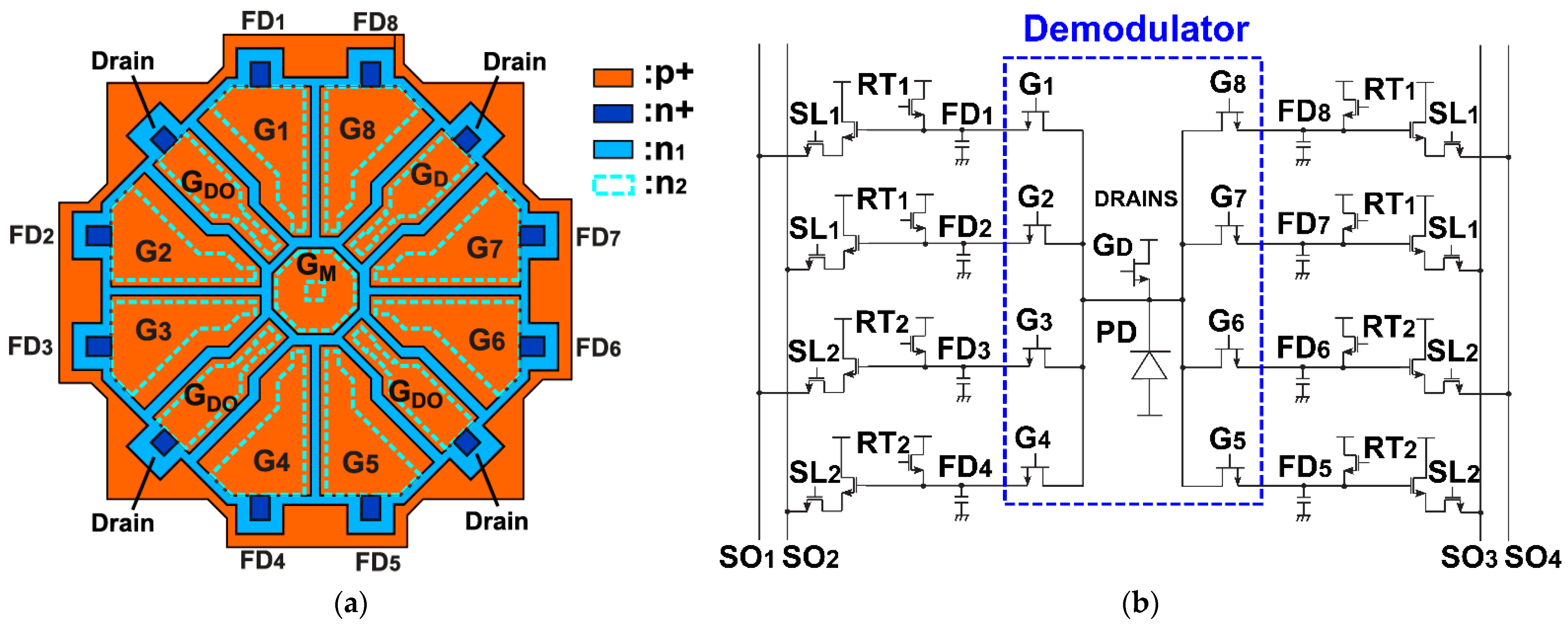
Figure 2. 8-tap demodulation pixel and the operations: (a) Top view of the 8-tap PND; (b) equivalent pixel readout circuits.
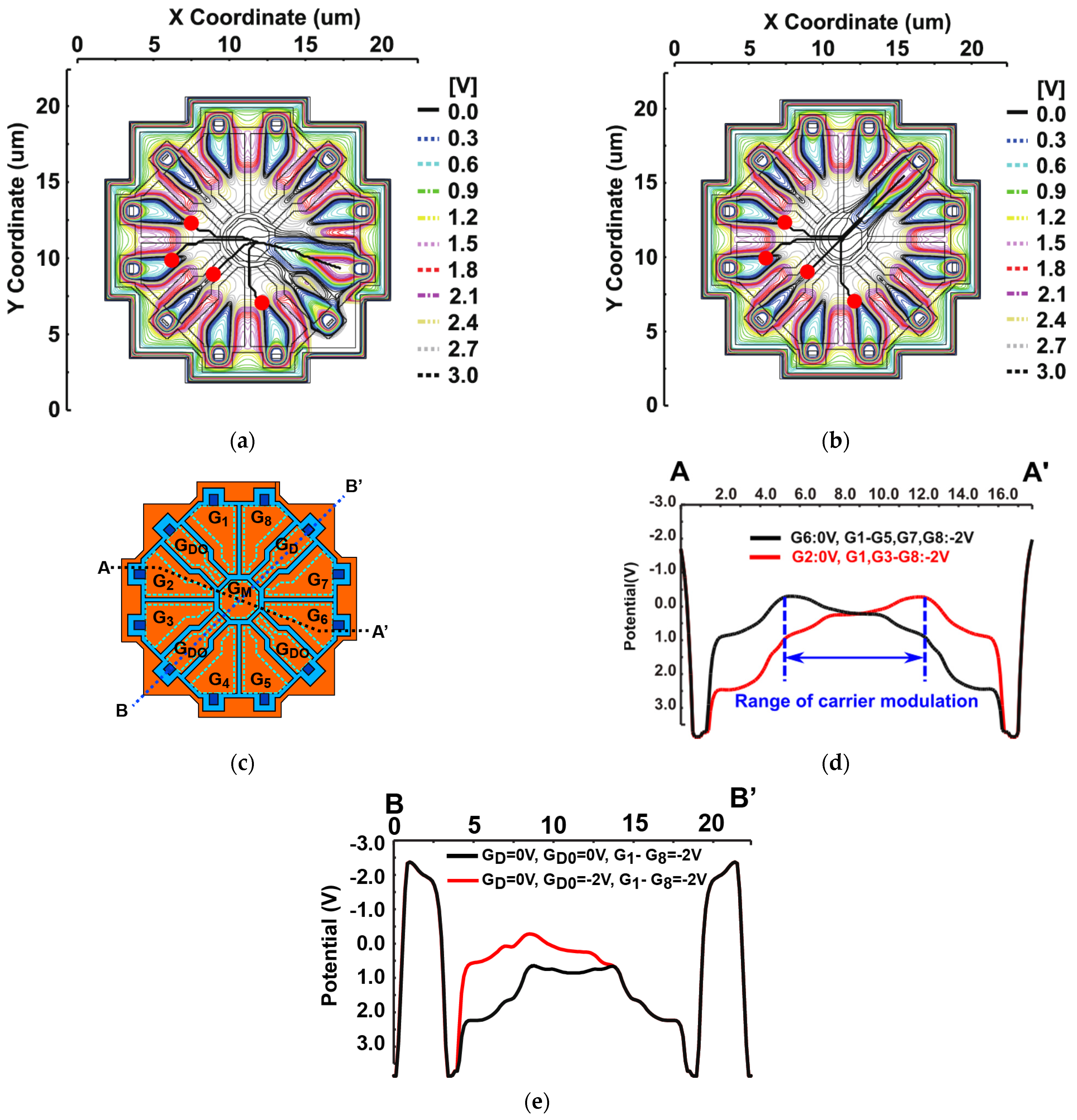
Figure 3. 3D device simulation results of the 8-tap PND: (a) X-Y 2D potential plot and carrier traces to transfer to G6; (b) X-Y 2D potential plot and carrier traces to transfer to GD; (c) demodulator top view; (d) 1D potential plot (A–A’) for carrier transfer to floating diffusions, FD6 and FD2; (e) 1D potential plot (B–B’) for carrier transferring to a drain through GD only (red line) and that for carrier transferring to a drain through GD and GDO (black line).
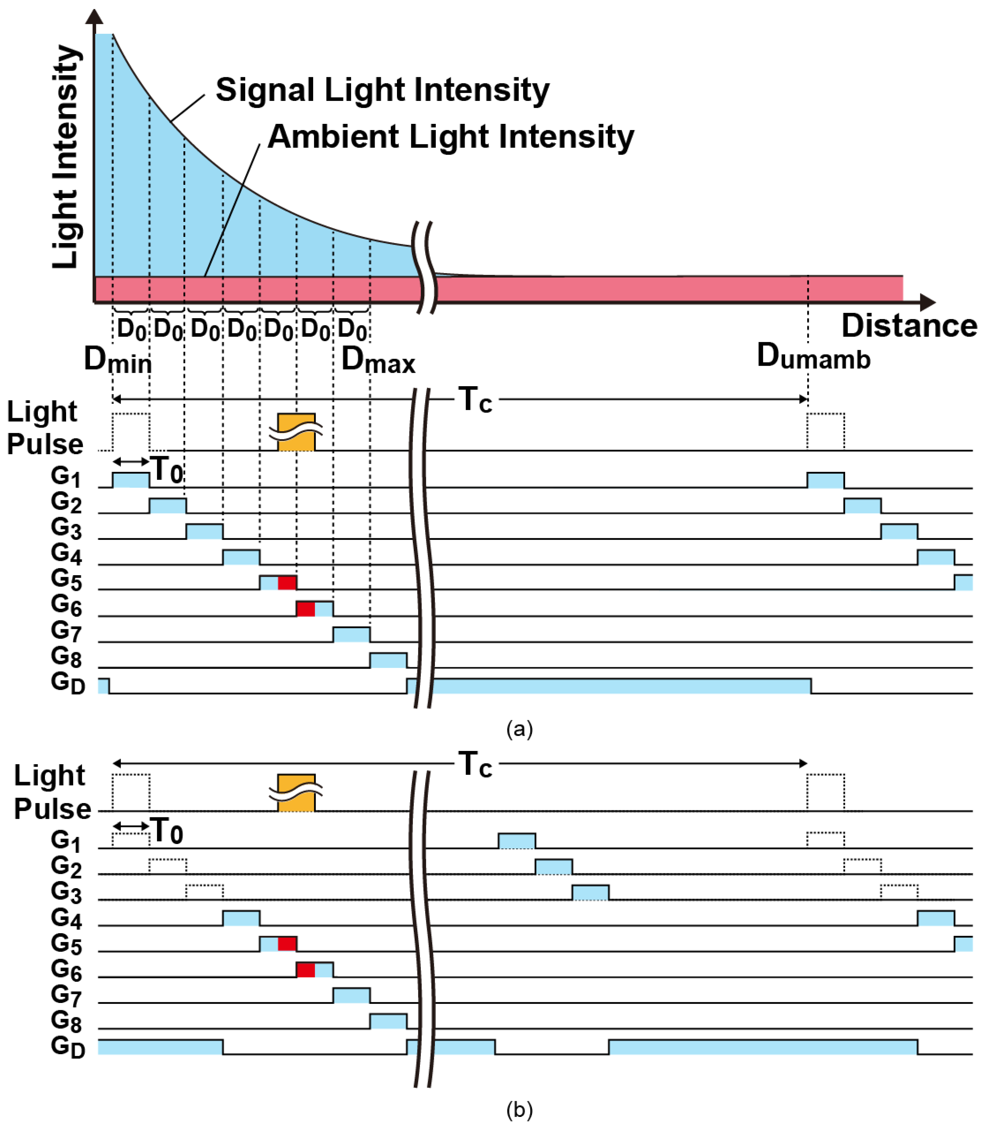
Figure 4. Gate timing and its correspondence to the depth range to be measured: (a) Gate timing when all the gates are activated in every cycle and its correspondence to the distance profile of the back-reflected light intensity; (b) Gate timing when G4–G8 are activated for signal light sampling and G1–G3 are activated for ambient light sampling.
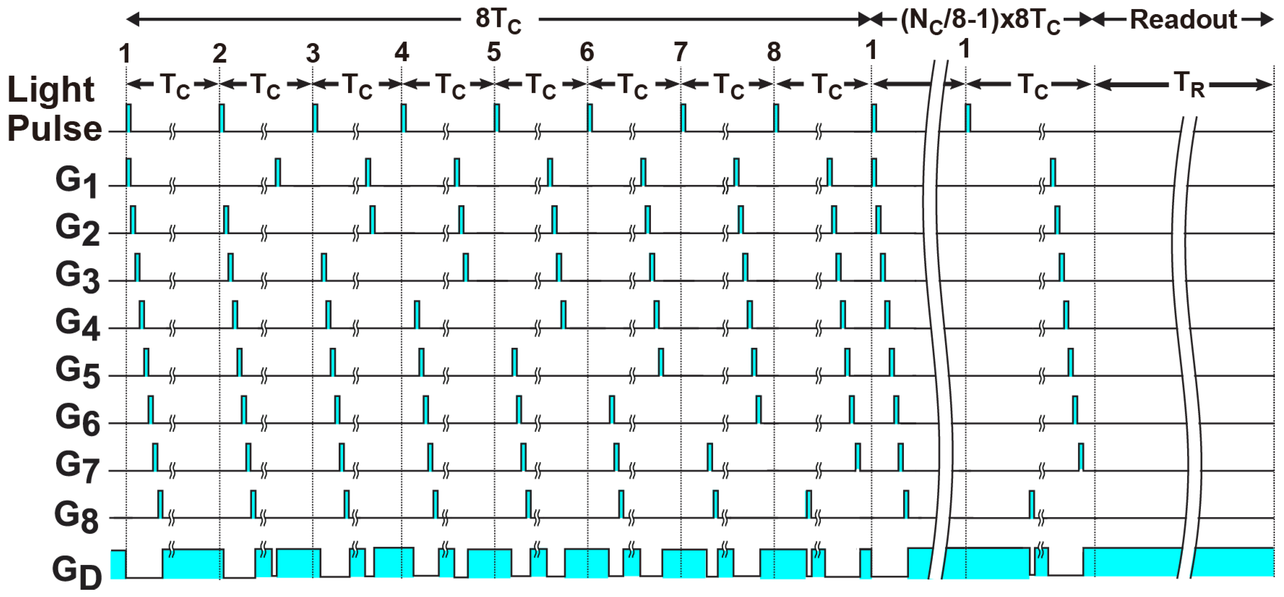
Figure 5. Example of the modified DATA timing diagram for cancelling ambient light.
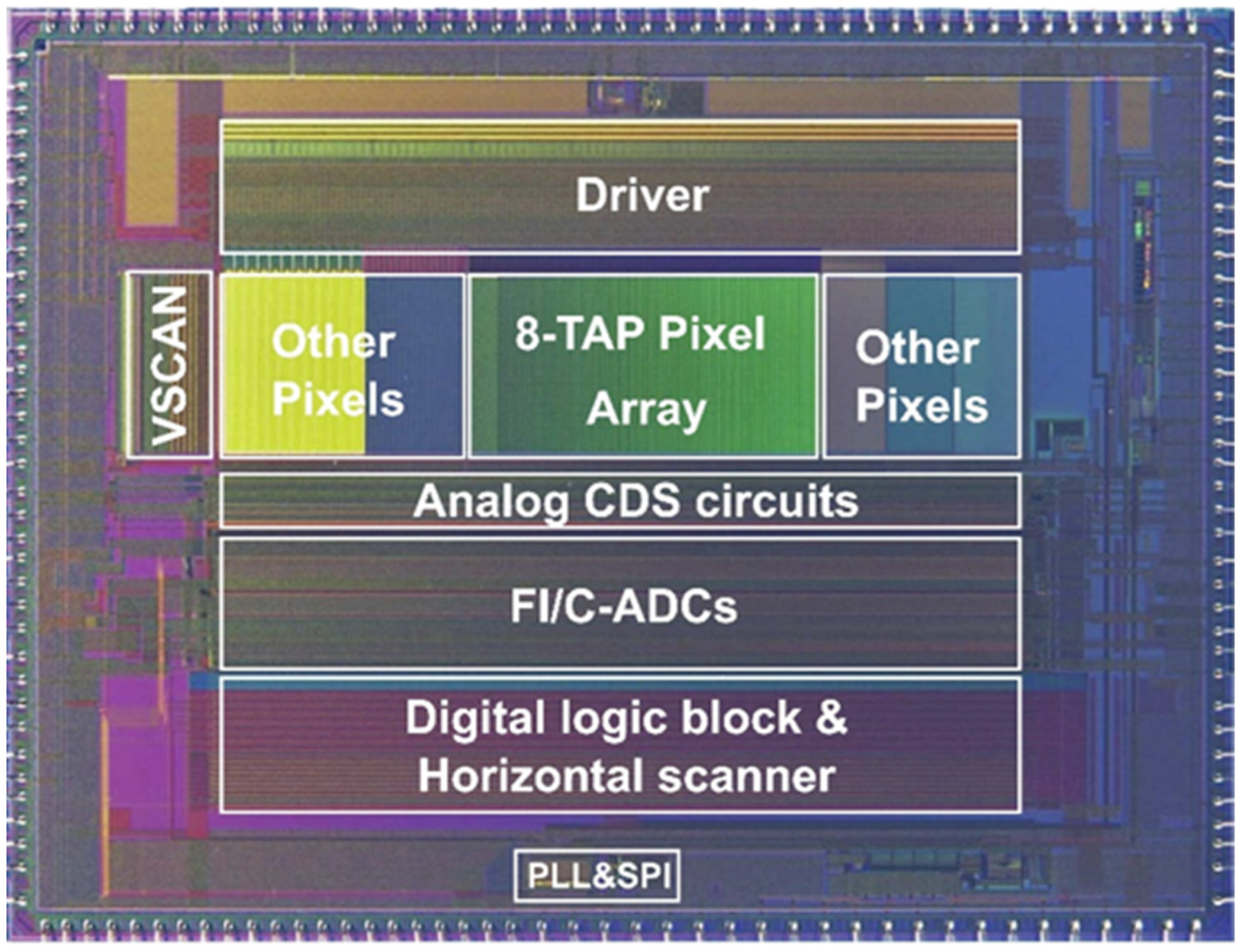
Figure 6. Chip micrograph.

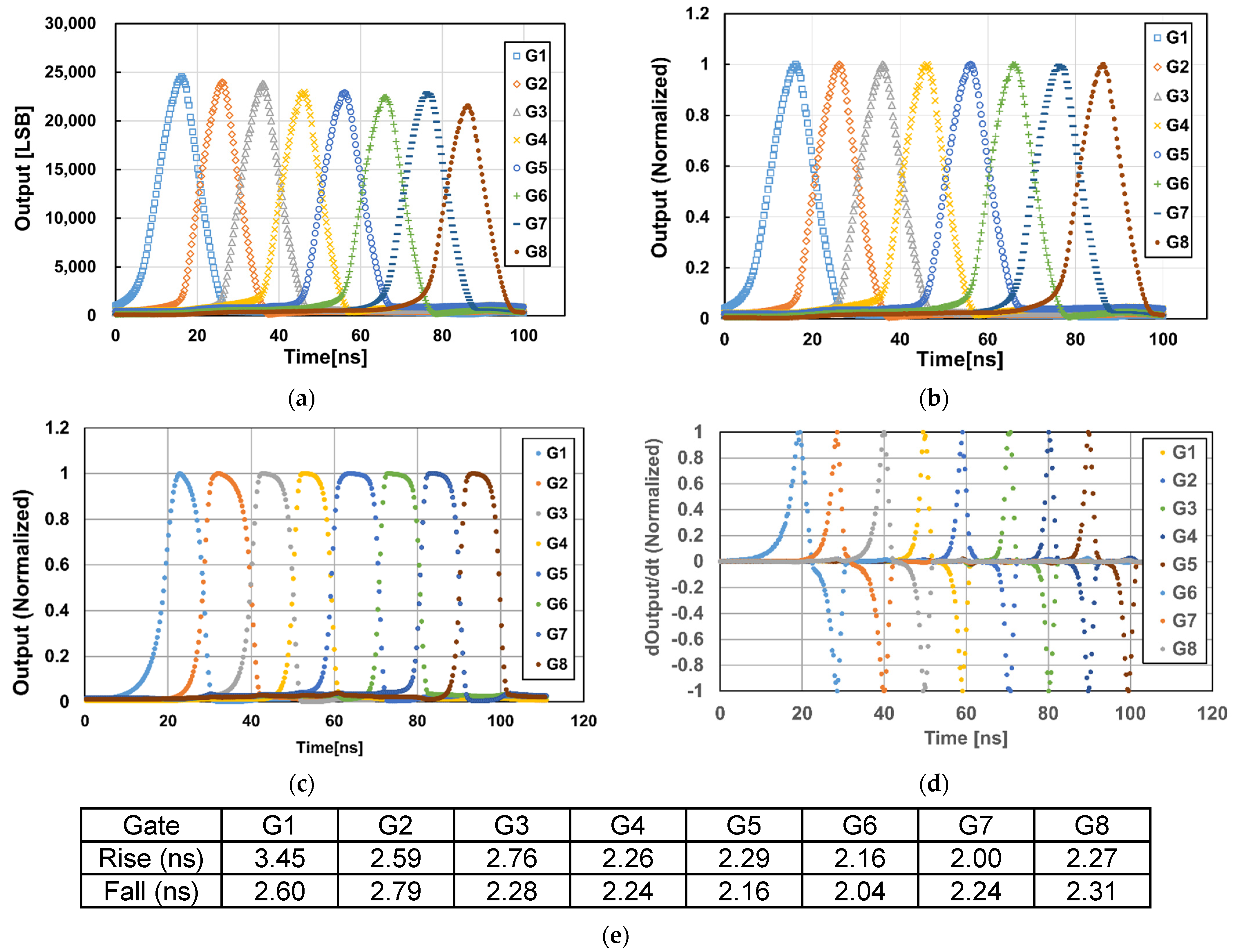
Figure 7. Response of the 8-tap outputs to the light pulse delay. (a) Response to Short Pulse (940 nm, T0 = 10 ns). (b) Response to Short Pulse (T0 = 10 ns, Normalized). (c) Response to Very Short Pulse (FWHM = 69 ps, 851 nm, Normalized). (d) Time Derivative of (c) by The Delay Time (Normalized). (e) FWHM of The Pixel Response to Very Short Pulse (FWHM = 69 ps) Measured with (d).
Great pixel lay-out, should be nominated for the "Most beautiful pixel lay-out of the year".
ReplyDelete