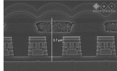
It uses copper process with 'De-Metallized Zone' (DMZ) structure in the pixel array to eliminate the reflective liner layers and boost the optical efficiency.
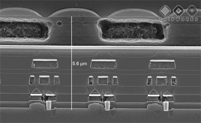
Use of copper allows reduction of the pixel optical thickness to just 3.7um, icluding color filter and (part of) microlens - quite an impressive achievement, see the picture below. Chipworks compares this with 5.6um of optical thickness for a previous generation Samsung Al-based 1.3MP sensor.
The older 1.3MP Samsung imager cross-section is below for comparison:
No comments:
Post a Comment
All comments are moderated to avoid spam and personal attacks.