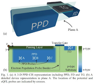
"In special cases such as time-of-flight imaging or large pinned photodiodes, the PPD potential well shape highly affects the charge transfer performance and should be engineered carefully. In the present work, a PPD structure named multi-level PPD is introduced and examined through simulation study. Moreover, a fast and effective way to analyze the pinning process for a lag-free design is introduced. It is concluded that the proposed PPD achieves fast and complete charge transfer without additional implementation masks or process steps. The proposed PPD is compared with a similar conventional rectangular pixel and 31% reduction in the charge transfer time is observed."


Missing a lot of important references starting from Kosonocky, Jarwal, Fraunhofer (Mahdi, Durini, Poklonskaya), STM (Tubert)...
ReplyDelete