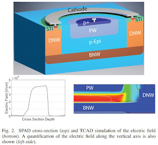
"Single-photon avalanche diodes (SPADs) have become the sensor of choice in many applications whenever high sensitivity, low noise, and sharp timing performance are required, simultaneously. Recently, SPADs designed in CMOS technology, have yielded moderately good performance in these parameters, but never equaling their counterparts fabricated in highly customized, non-standard technologies. The arguments in favor of CMOS-compatible SPADs were miniaturization, cost and scalability. In this paper, we present the first CMOS SPAD with performance comparable or better than that of the best custom SPADs, to date. The SPAD-based design, fully integrated in 180 nm CMOS technology, achieves a peak photon detection probability (PDP) of 55% at 480 nm with a very broad spectrum spanning from near ultraviolet (NUV) to near infrared (NIR) and a normalized dark count rate (DCR) of 0.2 cps/µm^2, both at 6V of excess bias. Thanks to a dedicated CMOS pixel circuit front-end, an afterpulsing probability of about 0.1% at a dead time of ∼3 ns were achieved. We designed three SPADs with a diameter of 25, 50, and 100 µm to study the impact of size on the timing jitter and to create a scaling law for SPADs. For these SPADs, a single-photon time resolution (SPTR) of 12.1 ps, 16 ps, and 27 ps (FWHM) was achieved at 6 V of excess bias, respectively. The SPADs operate in a wide range of temperatures, from -65◦C to 40◦C, reaching a normalized DCR of 1.6 mcps/µm^2 at 6 V of excess bias for the 25 µm at -65◦C."


This is a nice performing SPAD - congratulations! The measurements appear to have been thoroughly and rigorously performed.
ReplyDeleteHowever, the paper is weakened by an incomplete and cherry picked reference list to present the author's work in the best light, rather than just favorably. The authors also inadequately cite their SPAD design concept and it is inaccurately attributed to being "p-i-n" type regardless of this being impossible in the CMOS process given the implant scheme and the BV being too low for a truly intrinsic region. There are typographical errors in the summary table as well as it not being clear why some SPADs are N/A for FoMT.