https://www.photonics.com/Articles/New_Sensor_Materials_and_Designs_Deepen_SWIR/a68543
Some excerpts below:
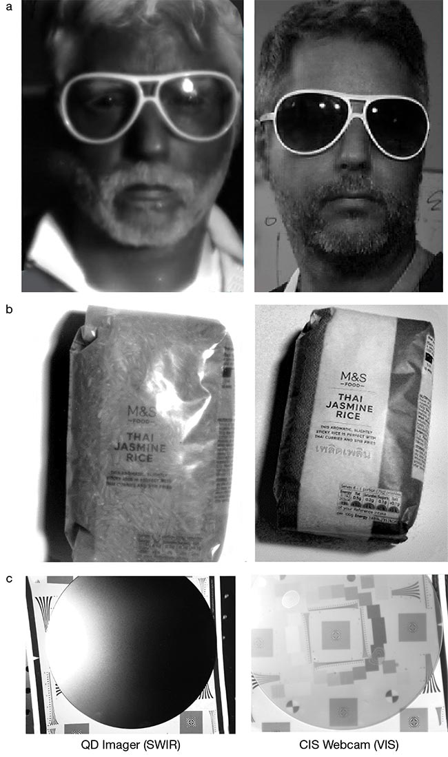
Cameras that sense wavelengths between 1000 and 2500 nm can often pick up details that would otherwise be hidden in images captured by conventional CMOS image sensors (CIS) that operate in the visible range. SWIR cameras can not only view details obscured by plastic sunglasses (a) and packaging (b), they can also peer through silicon wafers to spot voids after the bonding process (c). QD: quantum dot. Courtesy of mec.

A SWIR imaging forecast shows emerging sensor materials taking a larger share of the market, while incumbent InGaAs sees little gain, and the use of other materials grows at a faster rate. OPD: organic photodetector. Courtesy of IDTechEx.
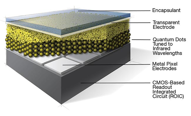
Quantum dots act as a SWIR photodetector if they are sized correctly. When placed on a readout circuit, they form a SWIR imaging sensor.
Silicon, the dominant sensor material for visible imaging, does not absorb SWIR photons without surface modification — and even then, it performs poorly. As a result, most SWIR cameras today use sensors based on indium gallium arsenide (InGaAs), ...
... sensors based on colloidal quantum dots (QDs) are gaining interest. The technology uses nanocrystals made of semiconductor materials, such as lead sulfide (PbS), that absorb in the SWIR. By adjusting the size of the nanocrystals used, sensor fabricators can create photodetectors that are sensitive from the visible to 2000 nm or even longer wavelengths.
... performance has steadily improved with the underlying materials and processing science, according to Pawel Malinowski, program manager of pixel innovations at imec. The organization’s third-generation QD-based image sensor debuted a couple of years ago with an efficiency of 45%. Newer sensors have delivered above 60% efficiency.
Fabricating QD photodiodes and sensors is also inexpensive because the sensor stack consists of a QD layer a few hundred nanometers thick, along with conducting, structural, and protective layers, Klem said. The stack goes atop a CMOS readout circuit in a pixel array. The technique can accommodate high-volume manufacturing processes and produce either large or small pixel arrays. Compared to InGaAs technology, QD sensors offer higher resolution and lower noise levels, along with fast response times.
Emberion, a startup spun out of Nokia, also makes QD-based SWIR cameras ... The quantum efficiency of these sensors is only 20% at 1800 nm... [but] ... at about half the price of InGaAs-based systems... .
[Another company TriEye is secretive about whether they use QD detectors but...] Academic papers co-authored by one of the company’s founders around the time that TriEye came into existence discuss pyramid-shaped silicon nanostructures that detect SWIR photons via plasmonic enhancement of internal photoemission.
a article from the 'other side of the problem', about progress in SWIR VCSEL: https://www.yolegroup.com/industry-news/trumpf-reports-breakthrough-in-industrializing-swir-vcsels-above-1300-nm/ - which could have a boost effect for SWIR image sensors
ReplyDeleteI guess author of first picture has inverted the two columns of first row.. facial hairs should be highly reflective and skin / eyes should appear dark.
ReplyDeleteI think the last row should have columns swapped. The transparent Silicon wafer shows up in the VIS column. The others match expected behavior for SWIR image.
Deletethis is not a si wafer but ir filter coated glas ;-)
DeleteI agree with "the last row should have columns swapped". The text under the picture shows as follows, " SWIR cameras can not only view details obscured by plastic sunglasses (a) and packaging (b), they can also peer through silicon wafers..".
ReplyDeleteAccording to the text description under those pictures, "WIR cameras can not only view details obscured by plastic sunglasses (a) and packaging (b), they can also peer through silicon wafers ..", I agree with the second last comment that the last row should have columns swapped.
ReplyDeleteJust for share.
ReplyDeletehttps://medium.com/@svogisan/short-wave-infrared-introduction-and-its-applications-17170d94f16d
show me your QE curve and i'll tell you who you are
ReplyDeleteI'll show you mine if you'll show me yours!
Delete