Saturday, January 30, 2021

Color Filters for 0.255um Pixels

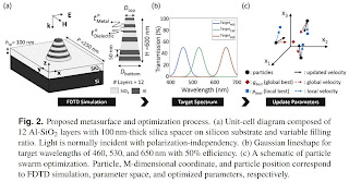
OSA Optics Express paper "Absorptive metasurface color filters based on hyperbolic metamaterials for a CMOS image sensor" by Jongwoo Hong, Hyunwoo Son, Changhyun Kim, Sang-Eun Mun, Jangwoon Sung, and Byoungho Lee from Seoul National University shows a possibility of a straight Bayer pattern with 0.255um pixels. By straight Bayer, I mean no 2x2, 3x3 or similar color grouping.

"Metasurface color filters (MCFs) have attracted considerable attention thanks to their compactness and functionality as a candidate of an optical element in a miniaturized image sensor. However, conventional dielectric and plasmonic MCFs that have focused on color purity and efficiency cannot avoid reflection in principle, which degrades image quality by optical flare. Here, we introduce absorptive-type MCFs through truncated-cone hyperbolic metamaterial absorbers. By applying a particle swarm optimization method to design multiple parameters simultaneously, the proposed MCF is theoretically and numerically demonstrated in perceptive color on CIELAB and CIEDE2000 with suppressed-reflection. Then, a color filter array is numerically proven in 255 nm of sub-pixel pitch."

The work is supported by the Samsung University R&D program.

Reference for Column-Parallel Sigma-Delta ADC

Ams and University of Madeira, Portugal, publish a MDPI paper "Reference Power Supply Connection Scheme for Low-Power CMOS Image Sensors Based on Incremental Sigma-Delta Converters" by Luis Miguel Carvalho Freitas and Fernando Morgado-Dias.

"Modern Complementary Metal-Oxide-Semiconductor (CMOS) image sensors, aimed to target low-noise and fast digital outputs, are fundamentally based on column-parallel structures, jointly designed with oversampling column converters. The typical choice for the employed column converters is the incremental sigma-delta structures, which intrinsically perform the correlated multiple sampling, creating an averaging effect over the system thermal noise when used in conjunction with 4T-pinned pixels. However, these types of column converters are known to be power-hungry, especially if the imaging device needs to target high frame rate levels as well. In this sense, the aim of this paper was to address the excess of power dissipation problem that arises from image sensors while employing oversampling high-order incremental converters, by means of using a different connection scheme to supply and to drive the required reference signals across the image sensor on-chip column converters. The proposed connection scheme revealed to be fully functional with no unwanted artifacts in the imager output response, allowing it to avoid 20% to 50% of the power dissipation, relative to the classical on-chip references generation and driving method. Furthermore, this solution allows for a much less complicated and less crowded printed circuit board (PCB) system."

Friday, January 29, 2021

Microsoft Partners with D3 Engineering, Leopard Imaging, and SICK to Deploy its ToF Technology in Industrial Applications

D3 Engineering announces its collaboration with Microsoft’s Azure Depth Platform program, setup to provide access to Microsoft’s ToF technology to a 3rd party ecosystem. This technology, developed for use in Hololens and Kinect, will allow D3 Engineering to create embedded spatial sensing systems, and deliver customized depth camera modules for camera makers and other OEMs. Further, by integrating with Microsoft’s Azure cloud-based learning and algorithms, the technology can be leveraged to increase effectiveness.

Microsoft’s advanced Time of Flight technology is highly desirable in a whole host of applications beyond the previous successful use cases in Gaming and Mixed Reality,” said Tom Mayo, Product Manager for Spatial Sensing at D3 Engineering. “D3 Engineering is excited to bring our extensive experience in embedded sensing systems design to provide solutions based on Microsoft’s technology. In our collaboration with Microsoft, we look forward to creating new, innovative sensing solutions for our customers.”  

D3 Engineering’s unique advantages include a U.S.-based design and engineering team as well as expertise in design and integration with ToF, radar, optics, and motion control.

We welcome D3 Engineering as Microsoft’s partner in solving customer challenges using our 3D sensing technology and Azure,” said Daniel Bar, head of business incubation for the Silicon & Sensor’s group at Microsoft. “Their experience in embedded system development and understanding of our platform combined with our Computer Vision and AI expertise will help democratize cloud connected 3D cameras.

PRNewswire: Leopard Imaging announces its collaboration with Microsoft's Azure Depth Platform program, aimed at democratizing cloud-connected 3D vision. In this collaboration, Leopard Imaging is developing 3D industrial cameras, which can securely connect with Azure Intelligent Edge and Intelligent Cloud platforms for a broad set of technologies and industry solutions. 

"Leopard Imaging is adopting Microsoft's ToF because of its clear advantages over competing technologies—providing high quality data with low artifacts, higher accuracy, lower jitter, and low power. By powering 3D camera solutions with Microsoft ToF, we want to stay competitive and continue to lead in this space. This collaboration will accelerate our growth and provide powerful solutions for our valued customers," says Bill Pu, President and Co-Founder of Leopard Imaging.

"Microsoft's collaboration with Leopard Imaging, as part of the Azure Depth Platform program, will light up 3D applications in new industrial scenarios and foster cloud connected innovation," said Cyrus Bamji, Partner Hardware Architect at Microsoft.

Earlier, Microsoft also announced a partnership with SICK on industrial ToF cameras:

SICK’s latest industrial 3DToF camera Visionary-T Mini is expected to be available for sales in early 2021. Visionary-T Mini incorporates a version of Microsoft’s 3D ToF technology with an extended dynamic range and a resolution of ~510 x 420 pixels. It will offer on-device processing infrastructure and tools not currently available with Azure Kinect DK, to include, but not limited to: 24/7 robustness, industrial interfaces, enhanced resolution with sharper depth images and enhanced depth quality. 

Cyrus Bamji also started a blog series about ToF technology.

Smartsens Starts IPO Preparations

SecuritiesDaily: The official website of the Shanghai Securities Regulatory Bureau disclosed that Smartsesn has submitted listing guidance and filing information and plans to IPO on the Science and Technology Innovation Board.  The announcement states that the company has started listing preparations on January 22, 2021.

Thursday, January 28, 2021

Worthy Survey?

University of Bridgeport, CT, and William Paterson University, NJ, publish a 50-page MDPI paper "CMOS Image Sensors in Surveillance System Applications" by Susrutha Babu Sukhavasi, Suparshya Babu Sukhavasi, Khaled Elleithy, Shakour Abuzneid, and Abdelrahman Elleithy. I wonder if somebody finds any use for this paper:
  • We have conducted the first state-of-the-art comprehensive survey on CIS from an applications’ perspective in different predominant fields, which was not done before.
  • A novel taxonomy has been introduced by us in which work is classified in terms of CIS models, applications, and design characteristics, as shown in Figure 1 and Appendix A Table A1.
  • We have noted the limitations and future directions and related works are highlighted.

Brigates Cancels its IPO Plans

HQEW reports that Brigates' (Ruixin Microelectronics) 1.347 billion yuan IPO plan has been scrapped.

"According to news on the official website of the Shanghai Stock Exchange on January 27, the Shanghai Stock Exchange has decided to terminate the review of the initial public offering of shares of Ruixin Microelectronics Co., Ltd. (hereinafter referred to as "Ruixin Micro") and listing on the Science and Technology Innovation Board."

Wednesday, January 27, 2021

trinamiX Introduces Behind OLED 3D Imaging Solution

NewswireToday, VentureBeat: trinamiX announces that its 3D imaging solution for secure face authentication now also works behind OLED displays of mobile devices.

trinamiX captures not only a 2D picture and a 3D depth map of the face, but also checks for “live skin” to recognize liveness in real-time. Spoofing the unlock system of a smartphone with a realistic full-face mask, 3D sculpture or even a detailed 2D printout becomes virtually impossible.

The hardware consists of just a standard CMOS sensor and a NIR light projector. The complete system can be mounted behind the smartphone display. The previously required smartphone notch is made obsolete.

We are very pleased to usher in this new era together with the smartphone OEMs,“ says Stefan Metz, Director 3D Imaging at trinamiX. “With our technology, users will no longer have to compromise as they benefit from the most secure privacy protection without sacrificing a user-friendly all-screen display.

Trinamix currently has 150 employees.

We focus on material classification for smartphones,” Metz said. “That means we can tell if it is human skin or something else, like plastic.


Eric Fossum, ON Semi, and Kodak Win Emmy Award

Dartmouth: US National Academy of Television announces 2021 Technology & Engineering Emmy Awards. The Award for Invention and Pioneering Development of Intra-Pixel Charge Transfer CMOS Image Sensors goes to:
  • Eric Fossum
  • ON Semiconductor
  • Eastman Kodak

Yole on Machine Vision Market

Yole Developpement publishes a report "The industrial vision market matters, and the ecosystem is reconfiguring."

"The supply chain of key image sensor components has centralized. Yole estimates that the top five camera players have 53% market share in industrial cameras. The top three image sensor players have more than 78% market share.

As software further improves camera function, leading players like Cognex and Basler have acquired software companies to strengthen their competitiveness. Smaller players are merging and gradually becoming larger players, for example TKH Group has merged many smaller camera players.

There have also been strong alliances, including upstream and downstream mergers to become giants, such as the recent Teledyne acquisition of FLIR. We have also seen some Chinese players come to the surface, such as Hikrobot, Huaray, and Imavision. They have grown by absorbing the technology of external players. As global manufacturing shifts to China, the Chinese machine vision market will be huge. Chinese machine vision players will therefore become important to watch in this market."

Gpixel Starts a Line of Charge-Domain TDI Sensors

Gpixel announces the first sensor in a new family of line scan CMOS sensors supporting true charge-domain time delay integration (TDI). GLT5009BSI is a BSI, TDI image sensor with 5 um pixels and 9072 pixel horizontal resolution. The sensor has two photosensitive bands, 256 stages and 32 stages respectively, enabling a HDR mode.

GLT5009BSI’s 5 um pixel provides a full well capacity of 16 ke- and noise of 8 e- which delivers more than 66 dB DR. Read out of the image data is achieved through 86 pairs of sub-LVDS channels at a combined maximum data rate of 72.58 Gbps. This output architecture supports line rates up to 600 kHz using 10-bit single band mode, 300 kHz using 12-bit single band mode.

The length of the photosensitive area is 45.36 mm and the sensor is assembled in a 269 pin uPGA package.

With the launch of the first sensor in the GLT family, Gpixel is able to address a new segment of applications requiring higher speed and more sensitivity than can be achieved with existing line scan products. We are excited to bring this high-end technology to our customers enabling them to address these demanding applications,” says Wim Wuyts, CCO of Gpixel.

GLT5009BSI engineering samples can be ordered now for delivery in March, 2021.

Tuesday, January 26, 2021

ams Announces 13.8MP and 8MP Global Shutter Sensors

BusinessWire: ams introduces the CSG family of image sensors for industrial vision equipment which achieves higher resolution at very high frame rates. The new CSG14K and CSG8K sensors are supplied in – respectively – a 1” or a 1/1.1” optical format.

The CSG14K is a global shutter image sensor that combines resolution of 13.8MP with high-speed operation: in 10-bit mode at full resolution, the sensor can capture images at a maximum rate of 140fps, and at 93.6fps in 12-bit mode. The CSG8K achieves even higher speeds of 231fps in 10-bit and 155fps in 12-bit mode at its full resolution of 8MP.

They are the first products to gain the benefits of a pixel design which is notable for its low noise and high sensitivity, plus HDR mode.

Peter Vandersteegen, Marketing Manager of the CMOS Image Sensors business line at ams, said: “AOI is a vital part of the quality control process in modern factories. By delivering a fast frame rate and higher resolution, the CSG image sensors provide a simple way for industrial camera manufacturers to upgrade the performance of their products, and to enable their cus-tomers to raise throughput, productivity and quality – all in a standard optical format.

The CSG sensors feature a sub-LVDS data interface like that of the ams CMV family of image sensors. Both sensors are supplied in a 20mm x 22mm LGA package, share the same footprint and pinout, and are software-compatible. The CSG14K has a 1:1 aspect ratio, and is ideal for use in C-mount, 29mm x 29mm industrial cameras. The CSG8K has a 16:9 aspect ratio, suita-ble for video. 

The CSG14K and CSG8K sensors are available for sampling.
Security Vulnerability of Rolling Shutter CMOS Sensors

Arxiv.org paper "They See Me Rollin': Inherent Vulnerability of the Rolling Shutter in CMOS Image Sensors" by Sebastian Köhler, Giulio Lovisotto, Simon Birnbach, Richard Baker, and Ivan Martinovic from Oxford University, UK, warns of security problem in machine vision systems relying on rolling shutter sensors.

"As a balance between production costs and image quality, most modern cameras use Complementary Metal-Oxide Semiconductor image sensors that implement an electronic rolling shutter mechanism, where image rows are captured consecutively rather than all-at-once.

In this paper, we describe how the electronic rolling shutter can be exploited using a bright, modulated light source (e.g., an inexpensive, off-the-shelf laser), to inject fine-grained image disruptions. These disruptions substantially affect camera-based computer vision systems, where high-frequency data is crucial in extracting informative features from objects.

We study the fundamental factors affecting a rolling shutter attack, such as environmental conditions, angle of the incident light, laser to camera distance, and aiming precision. We demonstrate how these factors affect the intensity of the injected distortion and how an adversary can take them into account by modeling the properties of the camera. We introduce a general pipeline of a practical attack, which consists of: (i) profiling several properties of the target camera and (ii) partially simulating the attack to find distortions that satisfy the adversary's goal. Then, we instantiate the attack to the scenario of object detection, where the adversary's goal is to maximally disrupt the detection of objects in the image. We show that the adversary can modulate the laser to hide up to 75% of objects perceived by state-of-the-art detectors while controlling the amount of perturbation to keep the attack inconspicuous. Our results indicate that rolling shutter attacks can substantially reduce the performance and reliability of vision-based intelligent systems."

Photonfocus Presents First Global Shutter UV Camera

Photonfocus unveils MV4-D1280U-H01-GT camera said to be the world's first global shutter UV camera. The 1.3MP BSI sensor is custom designed and has a  QE with > 40% in 170 - 800 nm band.


Thanks to TL for the pointer!

Monday, January 25, 2021

Next Generation EDOF

OSA Optics Express publishes a paper "Depth-of-field engineering in coded aperture imaging" by Mani Ratnam Rai and Joseph Rosen from Ben-Gurion University of the Negev, Israel.

"Extending the depth-of-field (DOF) of an optical imaging system without effecting the other imaging properties has been an important topic of research for a long time. In this work, we propose a new general technique of engineering the DOF of an imaging system beyond just a simple extension of the DOF. Engineering the DOF means in this study that the inherent DOF can be extended to one, or to several, separated different intervals of DOF, with controlled start and end points. Practically, because of the DOF engineering, entire objects in certain separated different input subvolumes are imaged with the same sharpness as if these objects are all in focus. Furthermore, the images from different subvolumes can be laterally shifted, each subvolume in a different shift, relative to their positions in the object space. By doing so, mutual hiding of images can be avoided. The proposed technique is introduced into a system of coded aperture imaging. In other words, the light from the object space is modulated by a coded aperture and recorded into the computer in which the desired image is reconstructed from the recorded pattern. The DOF engineering is done by designing the coded aperture composed of three diffractive elements. One element is a quadratic phase function dictating the start point of the in-focus axial interval and the second element is a quartic phase function which dictates the end point of this interval. Quasi-random coded phase mask is the third element, which enables the digital reconstruction. Multiplexing several sets of diffractive elements, each with different set of phase coefficients, can yield various axial reconstruction curves. The entire diffractive elements are displayed on a spatial light modulator such that real-time DOF engineering is enabled according to the user needs in the course of the observation. Experimental verifications of the proposed system with several examples of DOF engineering are presented, where the entire imaging of the observed scene is done by single camera shot."

LiDAR News: Levandowski, Aeva, DENSO, Ouster, Outsight, Argo, Valeo, Hyundai, Velodyne

World IP Review: The outgoing Trump administration has granted a full pardon to Anthony Levandowski, the former LiDAR head at Waymo, sentenced to 18 months in prison for stealing trade secrets.

In a memo, released on January 20, 2021, the administration says Levandowski “paid a significant price for his actions and plans to devote his talents to advance the public good.

It also cited a quote from the sentencing judge in the case in which he described Levandowski as a “brilliant, groundbreaking engineer that our country needs.

BusinessWire: Ouster and Outsight partner on the first integrated solution in the lidar industry with embedded pre-processing software. This plug-and-play system is designed to deliver real-time, processed 3D data and designed to be integrated into any application within minutes. The solution combines Ouster’s high-resolution digital lidar sensors with Outsight’s perception software which detects, classifies, and tracks objects without relying on machine learning.

ReutersDENSO partners with Aeva to develop next-generation sensing and perception systems. Together, the companies will advance FMCW LiDAR and bring it to the mass vehicle market.

MSNGroundTruthAutonomy: Argo.ai presents its new platform featuring 6 LiDARs and 11 cameras. Some of the versions even have a multi-storied LiDAR pyramid on the roof:


ETNews reports that Hyundai is contemplating using Valeo SCALA LiDAR in its first autonomous vehicle scheduled to release in 2022. The reason for choosing Valeo is quite interesting:

"This decision is likely based on the fact that Velodyne has yet to reach a level to mass-produce LiDAR sensors even though it is working with Hyundai Mobis, which invested $54.3 million (60 billion KRW) in Velodyne, on the development. 

Velodyne received an $50 million investment (3% stake) from Hyundai Mobis back in 2019. Although it stands at the top of the global market for LiDAR sensors, a supply of automotive LiDAR sensors for a research and development purpose is its only experience with automotive LiDAR sensors. It is reported that it has yet to reach Hyundai Motor Group’s requests due to its lack of experience with mass-production of automotive LiDAR sensors. Although it was planning to supply LiDAR sensors that will be used for a level 3 autonomous driving system, its plan is now facing a setback.

Velodyne is currently working with Hyundai Mobis at Hyundai Mobis’s Technical Center of Korea in Mabuk and is focusing on securing its ability to mass-produce automotive LiDAR sensors while having the sensors satisfy reliability that future cars require. The key is for Velodyne to minimize any different in qualities between products during mass-production

Valeo is the only company in the world that has succeeded in mass-producing automotive LiDAR sensors. It supplied “SCALA Gen. 1” to Audi for Audi’s full-size sedan “A8”. SCALA Gen. 1 is a 4-channel LiDAR sensor and it has a detection range of about 150 meters."

Sunday, January 24, 2021

International Image Sensor Society on LinkedIn

International Image Sensor Society (IISS) has opened a LinkedIn page. Please feel free to follow to be updated about the latest events and announcements:

12-ps Resolution Vernier Time-to-Digital Converter for SPAD Sensor

MDPI paper "A 13-Bit, 12-ps Resolution Vernier Time-to-Digital Converter Based on Dual Delay-Rings for SPAD Image Sensor" by Zunkai Huang, Jinglin Huang, Li Tian,Ning Wang, Yongxin Zhu, Hui Wang, and Songlin Feng from Shanghai Advanced Research Institute, Chinese Academy of Sciences, presents a fairly complex pixel.

"In this paper, we propose a novel high-performance TDC for a SPAD image sensor. In our design, we first present a pulse-width self-restricted (PWSR) delay element that is capable of providing a steady delay to improve the time precision. Meanwhile, we employ the proposed PWSR delay element to construct a pair of 16-stages vernier delay-rings to effectively enlarge the dynamic range. Moreover, we propose a compact and fast arbiter using a fully symmetric topology to enhance the robustness of the TDC. To validate the performance of the proposed TDC, a prototype 13-bit TDC has been fabricated in the standard 0.18-µm complementary metal–oxide–semiconductor (CMOS) process. The core area is about 200 µm × 180 µm and the total power consumption is nearly 1.6 mW. The proposed TDC achieves a dynamic range of 92.1 ns and a time precision of 11.25 ps. The measured worst integral nonlinearity (INL) and differential nonlinearity (DNL) are respectively 0.65 least-significant-bit (LSB) and 0.38 LSB, and both of them are less than 1 LSB. The experimental results indicate that the proposed TDC is suitable for SPAD-based 3D imaging applications."