Wednesday, November 30, 2022

IEDM 2022 (International Electron Devices Meeting)

IEDM conference will be held December 3-7, 2022 at the Hilton San Francisco Union Square. Starting December 12, the full conference will be on-demand. The full technical program is available here:

https://www.ieee-iedm.org/s/program2022-webiste-rev-002-779a.pdf

There are a couple of sessions of potential interest to the image sensors community.

Session 37: ODI - Silicon Image Sensors and Photonics
Wednesday, December 7, 1:30 p.m.

37.1 Coherent Silicon Photonics for Imaging and Ranging (Invited), Ali Hajimiri, Aroutin Khachturian, Parham Khial, Reza Fatemi, California Institute of Technology
Silicon photonics platform and their potential for integration with CMOS electronics present novel opportunities in applications such as imaging, ranging, sensing, and displays. Here, we present ranging and imaging results for a coherent silicon-imaging system that uses a two-path quadrature (IQ) approach to overcome optical path length mismatches.

37.2 Near-Infrared Sensitivity Enhancement of Image Sensor by 2 ND -Order Plasmonic Diffraction and the Concept of Resonant-Chamber-Like Pixel, Nobukazu Teranishi, Takahito Yoshinaga, Kazuma Hashimoto, Atsushi Ono, Shizuoka University
We propose 2 nd -order plasmonic diffraction and the concept of a resonant-chamber-like pixel to enhance the near-infrared (NIR) sensitivity of Si image sensors. Optical requirements for deep trench isolation are explained. In the simulation, Si absorptance as high as 49% at 940 nm wavelength for 3.25-µm-thick Si is obtained.

37.3 A SPAD Depth Sensor Robust Against Ambient Light: The Importance of Pixel Scaling and Demonstration of a 2.5µm Pixel with 21.8% PDE at 940nm, S. Shimada, Y. Otake, S. Yoshida, Y. Jibiki, M. Fujii, S. Endo, R. Nakamura, H. Tsugawa, Y. Fujisaki, K. Yokochi, J. Iwase, K. Takabayashi*, H. Maeda*, K. Sugihara*, K. Yamamoto*, M. Ono*, K. Ishibashi*, S. Matsumoto, H. Hiyama, and T. Wakano, Sony Semiconductor Solutions, *Sony Semiconductor Manufacturing
This paper presents scaled-down SPAD pixels to prevent PDE degradation under high ambient light. This study is carried out on Back-Illuminated structures with 3.3, 3.0, and 2.5µm pixel pitches. Our new SPAD pixels can achieve PDE at ?=940nm of over 20% and a peak of over 75%, even 2.5µm pixel.

37.4 3-Tier BSI CIS with 3D Sequential & Hybrid Bonding Enabling a 1.4um pitch,106dB HDR Flicker Free Pixel, F. Guyader, P. Batude*, P. Malinge, E.Vire, J. Lacord*, J. Jourdon, J. Poulet, L. Gay, F. Ponthenier*, S. Joblot, A. Farcy, L. Brunet*, A. Albouy*, C. Theodorou**, M. Ribotta*, D. Bosch*, E. Ollier*, D.Muller, M.Neyens, D. Jeanjean, T.Ferrotti, E.Mortini, J.G. Mattei, A. Inard, R. Fillon, F. Lalanne, F. Roy, E. Josse, STMicroelectronics, *CEA-Leti, Univ. Grenoble Alpes, **Univ. Grenoble Alpes, Univ. Savoie Mont Blanc, CNRS, Grenoble INP, IMEP-LAHC
A 3-tier CIS combining 3D Sequential Integration for the 2-tier pixel realization & Hybrid Bonding for the logic circuitry connection is demonstrated. Thin film pixel transistors are built above photo-gate without
congestion. Dual carrier collection 3DSI pixel offers an attractive dynamic range (106dB, Single Exposure) versus pixel pitch (1,4µm) trade-off

37.5 3-Layer Stacked Voltage-Domain Global Shutter CMOS Image Sensor with 1.8µm-Pixel-Pitch, Seung-Sik Kim, Gwi-Deok Ryan Lee, Sang-Su Park, Heesung Shim, Dae-Hoon Kim, Minjun Choi, Sangyoon Kim, Gyunha Park, Seung-Jae Oh, Joosung Moon, Sungbong Park, Sol Yoon, Jihye Jeong, Sejin Park, Sanggwon Lee, HaeJung Lee, Wonoh Ryu, Taehyoung Kim, Doowon Kwon, Hyuk Soon Choi, Hongki Kim, Jonghyun Go, JinGyun Kim, Seunghyun Lim, HoonJoo Na, Jae-kyu Lee, Chang-Rok Moon, Jaihyuk Song, Samsung Electronics
We developed a 1.8µm-pixel GS sensor which is suitable for mobile applications. Pixel shrink was possible by the 3-layer stacking structure with pixel-level Cu-to-Cu bonding and high-capacity DRAM capacitors. As a result, excellent performances were achieved i.e. -130dB, 1.8e-rms and 14ke- of PLS, TN and FWC, respectively.

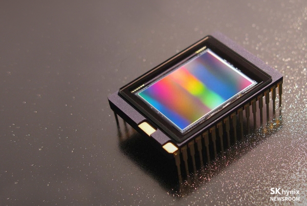
37.6 Advanced Color Filter Isolation Technolgy for Sub-Micron Pixel of CMOS Image Sensor, Hojin Bak, Horyeong Lee, Won-Jin Kim, Inho Choi, Hanjun Kim, Dongha Kim, Hanseung Lee, Sukman Han, Kyoung-In Lee, Youngwoong Do, Minsu Cho, Moung-Seok Baek, Kyungdo Kim, Wonje Park, Seong-Hun Kang, Sung-Joo Hong, Hoon-Sang Oh, and Changrock Song SK hynix Inc.
The novel color filter isolation technology, which adopts the air, the lowest refractive index material on the earth, as a major component of an optical grid for sub-micron pixels of CMOS image sensors, is presented. The image quality improvement was verified through the enhanced optical performance of the air-grid-assisted pixels.

37.7 A 140 dB Single-Exposure Dynamic-Range CMOS Image Sensor with In-Pixel DRAM Capacitor, Youngsun Oh, Jungwook Lim, Soeun Park, Dongsuk Yoo, Moosup Lim, Joonseok Park, Seojoo Kim, Minwook Jung, Sungkwan Kim, Junetaeg Lee, In-Gyu Baek, Kwangyul Ryu, Kyungmin Kim, Youngtae Jang, Min-SunKeel, Gyujin Bae, Seunghun Yoo, Youngkyun Jeong, Bumsuk Kim, Jungchak Ahn, Haechang Lee, Joonseo Yim, Samsung Electronics Co., Ltd.
A CMOS image sensor with a 2.1 µm pixel for automotive applications was developed. With a sub-pixel structure and a high-capacity DRAM capacitor, a single exposure dynamic range achieves 140 dB at 85, supporting LED flicker mitigation and blooming free. SNR stay above 23 dB at 105

Session 19: ODI - Photonic Technologies and Non-Visible Imaging
Tuesday, December 6, 2:15 p.m.

19.1 Record-low Loss Non-volatile Mid-infrared PCM Optical Phase Shifter based on Ge2Sb2Te 3S2, Y. Miyatake, K. Makino*, J. Tominaga*, N. Miyata*, T. Nakano*, M. Okano*, K. Toprasertpong, S. Takagi, M. Takenaka, The University of Tokyo, *National Institute of Advanced Industrial Science and Technology (AIST)
We propose a low-loss non-volatile PCM phase shifter operating at mid-infrared wavelengths using Ge 2Sb 2Te 3S2 (GSTS), a new selenium-free widegap PCM. The GSTS phase shifter exhibit the record-low optical loss for p phase shift of 0.29 dB/p, more than 20 times better than reported so far in terms of figure-of-merit.

19.2 Monolithic Integration of Top Si3N4-Waveguided Germanium Quantum-Dots Microdisk Light Emitters and PIN Photodetectors for On-chip Ultrafine Sensing, C-H Lin, P-Y Hong, B-J Lee, H. C. Lin, T. George, P-W Li, National Yang Ming Chiao Tung University
An ingenious combination of lithography and self-assembled growth has allowed accurate control over the geometric with high-temperature thermal stability. This significant fabrication advantage has opened up the 3D integration feasibility of top-SiN waveguided Ge photonics for on-chip ultrafine sensing and optical interconnect applications.

19.3 Colloidal quantum dot image sensors: a new vision for infrared (Invited), P. Malinowski, V. Pejovic*, E. Georgitzikis, JH Kim, I. Lieberman, N. Papadopoulos, M.J. Lim, L. Moreno Hagelsieb, N. Chandrasekaran, R. Puybaret, Y. Li, T. Verschooten, S. Thijs, D. Cheyns, P. Heremans*, J. Lee, imec,
*KULeuven
Short-wave infrared (SWIR) range carries information vital for augmented vision. Colloidal quantum dots (CQD) enable monolithic integration with small pixel pitch, large resolution and tunable cut-off wavelength, accompanied by radical cost reduction. In this paper, we describe the challenges to realize manufacturable CQD image sensors enabling new use cases.

19.4 Grating-resonance InGaAs narrowband photodetector for multispectral detection in NIR-SWIR region, J. Jang, J. Shim, J. Lim, G. C. Park*, J. Kim**, D-M Geum, S. Kim, Korea Advanced Institute of Science and Technology (KAIST), *Electronics and Telecommunications Research Institute (ETRI), **Korea Advanced Nano Fab Center (KANC)
We proposed grating-resonance narrowband photodetector for the wavelength selection functionality at the range of 1300~1700 nm. Based on parameters designed from the simulation, we fabricated an array of pixels to selectively detect different wavelengths. Our device showed great wavelength selectivity and tunability depending on grating design with a narrow FWHM.

19.5 Alleviating the Responsivity-Speed Dilemma of Photodetectors via Opposite Photogating Engineering with an Auxiliary Light Source beyond the Chip, Y. Zou, Y. Zeng, P. Tan, X. Zhao, X. Zhou, X. Hou, Z. Zhang, M. Ding, S. Yu, H. Huang, Q. He, X. Ma, G. Xu, Q. Hu, S. Long, University of Science and Technology of China
The dilemma between responsivity and speed limits the performance of photodetectors. Here, opposite photogating engineering was proposed to alleviate this dilemma via an auxiliary light source beyond the chip. Based on a WSe 2/Ga 2O3 JFET, a >103 times faster speed towards deep ultra-violet has been achieved with negligible sacrifice of responsivity.

19.6 Experimental Demonstration of the Small Pixel Effect in an Amorphous Photoconductor using a Monolithic Spectral Single Photon Counting Capable CMOS-Integrated Amorphous-Selenium Sensor, R. Mohammadi, P. M. Levine, K. S. Karim, University of Waterloo
We directly demonstrate, for the first time, the small pixel effect in an amorphous material, a-Se. The results are also the first demonstration of the transient response of a-Se monolithically combined with a CMOS, with and without SPE, and the first aSe/CMOS PHS results, offering a-Se/CMOS for photon counting applications.

Monday, November 28, 2022

Harvest Imaging Forum April 5 and 6, 2023

https://harvestimaging.com/forum_introduction_2023_new.php

After the Harvest Imaging forums during the last decade, a next and nineth one will be organized on April 5 & 6, 2023 in Delft, the Netherlands. The basic intention of the Harvest Imaging forum is to have a scientific and technical in-depth discussion on one particular topic that is of great importance and value to digital imaging. The forum 2023 will again be organized in a hybrid form:

  • You can attend in-person and can benefit in the optimal way of the live interaction with the speakers and audience,
  • There will be also a live broadcast of the forum, still interactions with the speakers through a chat box will be made possible,
  • Finally the forum also can be watched on-line at a later date.

The 2023 Harvest Imaging forum will deal with a single topic from the field of solid-state imaging and will have only one world-level expert as the speaker.

Register here: https://harvestimaging.com/forum_registration_2023_new.php


"Imaging Beyond the Visible"
Prof. dr. Pierre MAGNAN (ISAE-SUPAERO, Fr)
 

Abstract:
Two decades of intensive and tremendous efforts have pushed the imaging capabilities in the visible domain closer to physical limits. But also extended the attention to new areas beyond visible light intensity imaging. Examples can be found either to higher photon energy with appearance of CMOS Ultra-Violet imaging capabilities or even to other light dimensions with Polarization Imaging possibilities, both in monolithic form suitable to common camera architecture.

But one of most active and impressive fields is the extension of interest to the spectral range significantly beyond the visible, in the Infrared domain. Special focus is put on the Short Wave Infrared (SWIR) used in the reflective imaging mode but also the Thermal Infrared spectral range used in self-emissive ‘thermal’ imaging mode in Medium Wave Infrared (MWIR) and Long Wave Infrared (LWIR). Initially mostly motivated for military and scientific applications, the use of these spectral domains have now met new higher volume applications needs.

This has been made possible thanks to new technical approaches enabling cost reduction stimulated by the efficient collective manufacturing process offered by the microelectronics industry. CMOS, even no more sufficient to address alone the non- visible imaging spectral range, is still a key part of the solution.

The goal of this Harvest Imaging forum is to go through the various aspects of imaging concepts, device principles, used materials and imager characteristics to address the beyond-visible imaging and especially focus on the infrared spectral bands imaging.

Emphasis will be put on the material used for both detection :

  • Germanium, Quantum Dots devices and InGaAs for SWIR,
  •  III-V and II-VI semiconductors for MWIR and LWIR
  •  Microbolometers and Thermopiles thermal imagers

Besides the material aspects, also attention will be given to the associated CMOS circuits architectures enabling the imaging arrays implementation, both at the pixel and the imager level.
A status on current and new trends will be provided.
 

Bio:
Pierre Magnan graduated in E.E. from University of Paris in 1980. After being a research scientist involved in analog and digital CMOS design up to 1994 at French Research Labs, he moved in 1995 to CMOS image sensors research at SUPAERO (now ISAE-SUPAERO) in Toulouse, France. The latter is an Educational and Research Institute funded by the French Ministry of Defense. Here Pierre was involved in setting up and growing the CMOS active-pixels sensors research and development activities. From 2002 to 2021, as a Full Professor and Head of the Image Sensor Research Group, he has been involved in CMOS Image Sensor research. His team worked in cooperation with European companies (including STMicroelectronics, Airbus Defense& Space, Thales Alenia Space and also European and French Space Agencies) and developed custom image sensors dedicated to space instruments, extending in the last years the scope of the Group to CMOS design for Infrared imagers.
In 2021, Pierre has been nominated Emeritus Professor of ISAE-Supaero Institute where he focuses now on Research within PhD work, mostly with STMicroelectronics.

Pierre has supervised more than 20 PhDs candidates in the field of image sensors and co-authored more than 80 scientific papers. He has been involved in various expertise missions for French Agencies, companies and the European Commission. His research interests include solid-state image sensors design for visible and non-visible imaging, modelling, technologies, hardening techniques and circuit design for imaging applications.

He has served in the IEEE IEDM Display and Sensors subcommittee in 2011-2012 and in the International Image Sensor Workshop (IISW) Technical Program Committee, being the General Technical Chair of 2015 IISW. He is currently a member of the 2022 IEDM ODI sub-committee and the IISW2023 Technical Program Committee.


Friday, November 25, 2022

Himax Technologies, Inc. Announces Divestiture of Emza Visual Sense Subsidiary

Link:  https://www.globenewswire.com/news-release/2022
/10/28/2543724/8267/en/Himax-Technologies-Inc-Announces-Divestiture-of-Emza-Visual-Sense-Subsidiary.html


TAINAN, Taiwan, Oct. 28, 2022 (GLOBE NEWSWIRE) -- Himax Technologies, Inc. (Nasdaq: HIMX) (“Himax” or “Company”), a leading supplier and fabless manufacturer of display drivers and other semiconductor products, today announced that it has divested its wholly owned subsidiary Emza Visual Sense Ltd. (“Emza”), a company dedicated to the development of proprietary vision machine-learning algorithms. Following the transaction, Himax will continue to partner with Emza. The divestiture will not affect the existing business with the leading laptop customer where Himax continues to be the supplier for the leading-edge ultralow power AI processor and always-on CMOS image sensor.

WiseEyeTM, Himax’s total solution for ultralow power AI image sensing, includes Himax proprietary AI processors, CMOS image sensors, and CNN-based machine-learning AI algorithms, all featuring unique characteristics of ultralow power consumption. For the AI algorithms, Himax has historically adopted a business model where it not only develops its own solutions through an in-house algorithm team and Emza, a fully owned subsidiary before the divestiture, but also partners with multiple third-party AI algorithm specialists as a way to broaden the scope of application and widen the geographical reach. Moving forward, the AI business model will be unchanged where the Company will continue to develop its own algorithms and work with third-party algorithms partners, including Emza.

The Company continues to collaborate with its ecosystem partners to jointly make the WiseEye AI solution broadly accessible to the market, aiming to scale up adoption in numerous relatively untapped end-point AI markets. Tremendous progress has been made so far in areas such as laptop, desktop PC, automatic meter reading, video conference device, shared bike parking, medical capsule endoscope, automotive, smart office, battery cam and surveillance, among others. Additionally, Himax is committed to strengthening its WiseEye product roadmap while retaining its leadership position in ultralow power AI processor and image sensor. By targeting even lower power consumption and higher AI inference performance that leverage integral optimization from hardware to software, the Company believes it can capture the vast end-point AI opportunities presented ahead.

Wednesday, November 23, 2022

SK Hynix developing AI powered image sensor

From: https://www.thelec.net/news/articleView.html?idxno=4281


SK Hynix was developing a new CMOS image sensor (CIS) that uses neural network technology, TheElec has learned. The South Korean memory giant is planning to embed an AI accelerator into the CIS, sources said. The accelerator itself is based on SRAM combined with a microprocessor --- also called in-memory computing. The AI-powered CIS will be able to recognize information related to the subject of the image, while the image was being saved as data. For example, the CIS will be able to recognize the owner of the smartphone when it is used on a front camera. Most current devices have the CIS and the face-recognizing feature separate. Having the CIS do it on its own can save time and conserve the power of the device. SK Hynix has recently verified the design and field programmable gate array of the CIS. The company is also planning to develop an AI accelerator that uses non-volatile memory instead of the volatile SRAM. SK Hynix is a very small player in the CIS field. According to Strategy Analytics, Sony controlled 44% of the market during the first half of the year followed by Samsung’s 30%. Omivision had a 9% market share. The remaining three companies, which include SK Hynix, controlled 17% together. SK Hynix is currently supplying its high-resolution CIS to Samsung; last year it supplied a 13MP CIS for the Galaxy Z Fold 3. It is supplying 50MP CIS for the Galaxy A series this year. However, CIS companies are focusing on strengthening other features of the CIS besides resolution. They are reaching the limits of making the pixels smaller. Pixels absorb less light and the signals are smaller when they become too small, obscuring the resolution of the images.


Monday, November 21, 2022

Sony to make self-driving sensors that need 70% less power

From: https://asia.nikkei.com/Business/Automobiles/Sony-to-make-self-driving-sensors-that-need-70-less-power

Sony is developing its own electric vehicles. (Asia Nikkei)
July 19, 2022


TOKYO -- Sony Group will develop a new self-driving sensor that uses 70% less electricity, helping to reduce autonomous systems' voracious appetite for power and extend the range of electric vehicles.
The sensor, made by Sony Semiconductor Solutions, will be paired with new software to be developed by Sompo Holdings-backed startup Tier IV with the goal of cutting the amount of power used by EV onboard systems by 70%. The companies hope to achieve Level 4 technology, allowing cars to drive themselves under certain conditions, by 2030.


Electric vehicles will make up 59% of new car sales globally in 2035, the Boston Consulting Group predicts. Over 30% of trips 5 km and longer are expected to be made in self-driving cars, which rely on large numbers of sensors and cameras and transmit massive amounts of data.


Existing autonomous systems are said to use as much power as thousands of microwave ovens, hindering improvements in the driving range of EVs. Combined with the drain from air conditioning and other functions, EVs could end up with a range at least 35% smaller than on paper, according to Japan's Ministry of Economy, Trade and Industry. If successful, Sony's new sensors would limit this impact to around 10%.


Sony plans to lower the amount of electricity needed in self-driving systems through edge computing, processing as much data as possible through AI-equipped sensors and software on the vehicles themselves instead of transmitting it to external networks. This approach is expected to shrink communication lags as well, making the vehicles safer. 

[Thanks to the anonymous blog comment for sharing the article text.]


Friday, November 18, 2022

InP Market Expanding, Proximity Sensor on iPhone 14, Depth Sensing Issues on iPhone 13

From Electronics Weekly and Yole:

https://www.electronicsweekly.com/news/business/inp-moving-into-consumer-2022-10/

https://www.yolegroup.com/strategy-insights/apple-and-the-compound-semi-industry-the-story-begins/ 

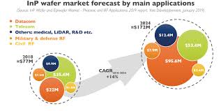
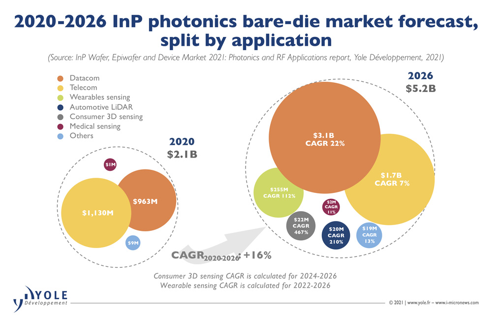
The InP device market is expanding from traditional datacom and telecom towards the consumer reaching about $5.6 billion by 2027, says Yole Developpement.


Datacom and telecom applications are the traditional markets for InP.Land will continue to grow, but the biggest growth driver – with a 37% CAGR between 2021 and 2027 – will be consumer.
The InP supply chain is fragmented, though it is dominated by two vertically integrated American players: Coherent (formerly II-VI) and Lumentum.


The InP supply chain will need more investment with the rise of the consumer applications.
The migration to higher data rates, lower power consumption within data centres, and the deployment of 5G base stations will drive the development and growth of optical transceiver technology in the coming years.
 

As an indispensable building block for high-speed and long-range optical transceivers, InP laser diodes remain the best choice for telecom & datacom photonic applications.
This growth is driven by high volume adoption of high-data-rate modules, above 400G, by big cloud services and national telecom operators requiring increased fiber-optic network capacity.
 

With that in mind, the InP market, long dominated by datacom and telecom applications, is expected grow from $2.5 billion in 2021 to around $5.6 billion in 2027.
 

Yole Intelligence has developed a dedicated report to provide a clear understanding of the InP-based photonics and RF industries. In its InP 2022 report, the company, part of Yole Group, provides a comprehensive view of the InP markets, divided into photonics and RF sectors. It includes market forecasts, technology trends, and supply chain analysis. This updated report covers the markets from wafer to bare die for photonics applications and from wafer to epiwafer for RF applications by volume and revenue.
 

“There has been a lot of speculation on the penetration of InP in consumer applications,” says Yoke’s Ali Jaffal, “the year 2022 marks the beginning of this adoption. For smartphones, OLED displays are transparent at wavelengths ranging from around 13xx to 15xx nm”.
 

OEMs are interested in removing the camera notch on mobile phone screens and integrating the 3D-sensing modules under OLED displays. In this context, they are considering moving to InP EELs to replace the current GaAs VCSELs . However, such a move is not straightforward from cost and supply perspectives.
 

Yole Intelligence noted the first penetration of InP into wearable earbuds in 2021. Apple was the first OEM to deploy InP SWIR proximity sensors in its AirPods 3 family to help differentiate between skin and other surfaces.
 

This has been extended to the iPhone 14 Pro family. The leading smartphone player has changed the aesthetics of its premium range of smartphones, the iPhone 14 Pro family, reducing the size of the notch at the top of the screen to a pill shape.


To achieve this new front camera arrangement, some other sensors, such as the proximity sensor, had to be placed under the display. Will InP penetration continue in other 3D sensing modules, such as dot projectors and flood illuminators? Or could GaAs technology come back again with a different solution for long-wavelength lasers?
 

The impact of Apple adding such a differentiator to its product significantly affects companies in its supply chain, and vice versa.
 

Traditional GaAs suppliers for Apple’s proximity sensors could switch from GaAs to InP platforms since both materials could share similar front-end processing tools.
 

Yole Intelligence certainly expects to see new players entering the InP business as the consumer market represents high volume potential.
 

In addition, Apple’s move could trigger the penetration of InP into other consumer applications, such as smartwatches and automotive LiDAR with silicon photonics platforms.


In other Apple iPhone related news:

The True Depth camera on the iPhone 13 seems to be oversmoothing at distances over 20cm:


Wednesday, November 16, 2022

CellCap3D: Capacitance Calculations for Image Sensor Cells

Sequoia's CellCap3D is a software tool specifically designed for the capacitance matrix calculation of image sensor cells. It is fast, accurate and easy to use.


Please contact SEQUOIA Design Systems, Inc. for further details at info@sequoiadesignsystems.com

Monday, November 14, 2022

Videos du jour for Nov 14, 2022

Graphene Flagship (https://graphene-flagship.eu/) spearhead project AUTOVISION is developing a new high-resolution image sensor for autonomous vehicles, which can detect obstacles and road curvature even in extreme and difficult driving conditions.


SPAD and CIS camera fusion for high resolution high dynamic range passive imaging (IEEE/CVF WACV 2022) Authors: Yuhao Liu (University of Wisconsin-Madison)*; Felipe Gutierrez-Barragan (University of Wisconsin-Madison); Atul N Ingle (University of Wisconsin-Madison); Mohit Gupta ("University of Wisconsin-Madison, USA "); Andreas Velten (University of Wisconsin - Madison) Description: Reconstruction of high-resolution extreme dynamic range images from a small number of low dynamic range (LDR) images is crucial for many computer vision applications. Current high dynamic range (HDR) cameras based on CMOS image sensor technology rely on multiexposure bracketing which suffers from motion artifacts and signal-to-noise (SNR) dip artifacts in extreme dynamic range scenes. Recently, single-photon cameras (SPCs) have been shown to achieve orders of magnitude higher dynamic range for passive imaging than conventional CMOS sensors. SPCs are becoming increasingly available commercially, even in some consumer devices. Unfortunately, current SPCs suffer from low spatial resolution. To overcome the limitations of CMOS and SPC sensors, we propose a learning-based CMOS-SPC fusion method to recover high-resolution extreme dynamic range images. We compare the performance of our method against various traditional and state-of-the-art baselines using both synthetic and experimental data. Our method outperforms these baselines, both in terms of visual quality and quantitative metrics.


System Semiconductor Image Sensor Explained | 'All About Semiconductor' by Samsung Electronics


tinyML neuromorphic engineering discussion forum:

Neuromorphic Event-based Vision
Christoph POSCH
CTO
PROPHESEE


New Architecture for Visual AI, Oculi Technology Enables Edge Solutions At The Speed Of Machines With The Efficiency of Biology
Charbel RIZK,
Founder CEO
Oculi Inc.


Roman Genov, University of Toronto
Fast Field-Programmable Coded Image Sensors for Versatile Low-Cost Computational Imaging Presented through the Chalk Talks series of the Institute for Neural Computation (UC San Diego)
08/05/22


Saturday, November 12, 2022

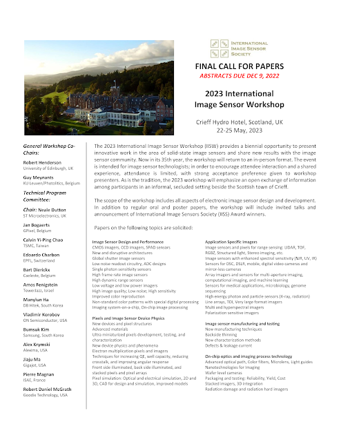
2023 International Image Sensor Workshop (IISW): Final Call for Papers Available

The final call for papers for 2023 IISW is now available: https://imagesensors.org/2023-international-image-sensor-workshop/

To submit
an abstract, please go to: https://cmt3.research.microsoft.com/IISW2023

The deadline for abstract submission is 11:59pm, Friday December 9th, 2022 (GMT).

The 2023 International Image Sensor Workshop (IISW) provides a biennial opportunity to present innovative work in the area of solid-state image sensors and share new results with the image sensor community. Now in its 35th year, the workshop will return to an in-person format. The event is intended for image sensor technologists; in order to encourage attendee interaction and a shared experience, attendance is limited, with strong acceptance preference given to workshop presenters. As is the tradition, the 2023 workshop will emphasize an open exchange of information among participants in an informal, secluded setting beside the Scottish town of Crieff.

The scope of the workshop includes all aspects of electronic image sensor design and development. In addition to regular oral and poster papers, the workshop will include invited talks and announcement of International Image Sensors Society award winners.


Friday, November 11, 2022

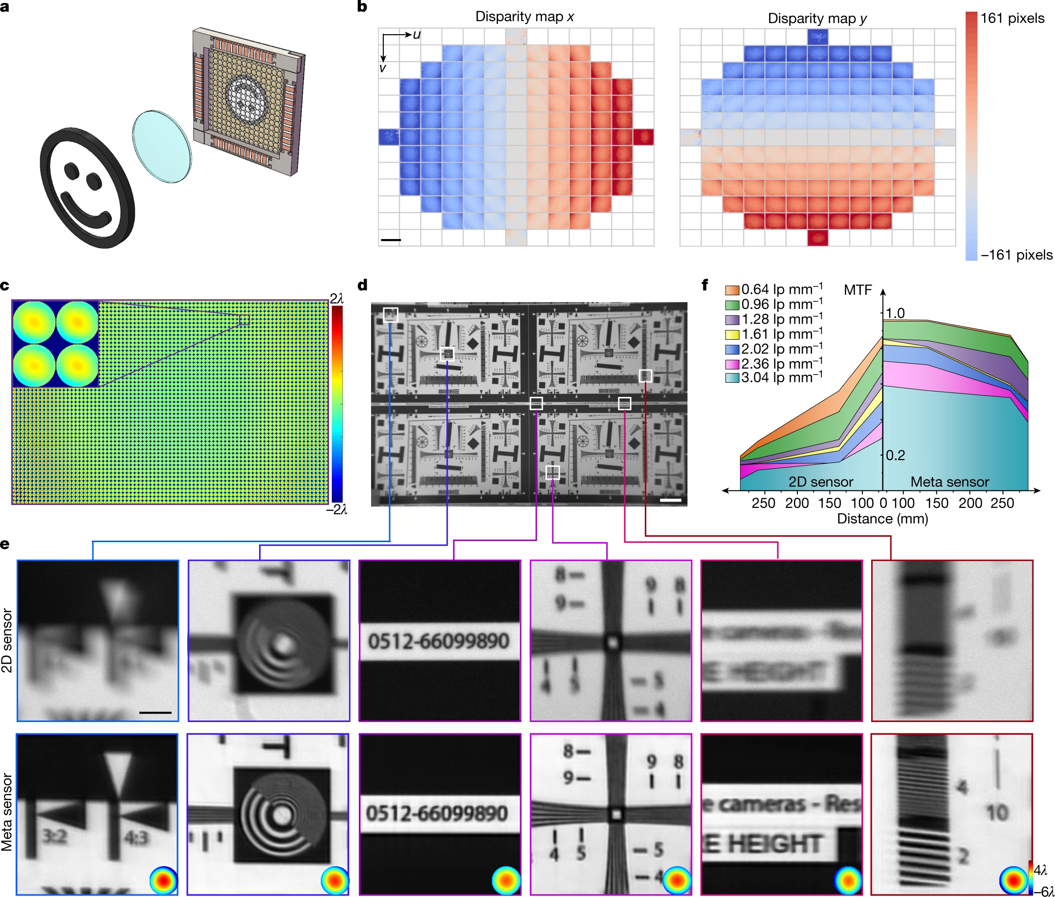
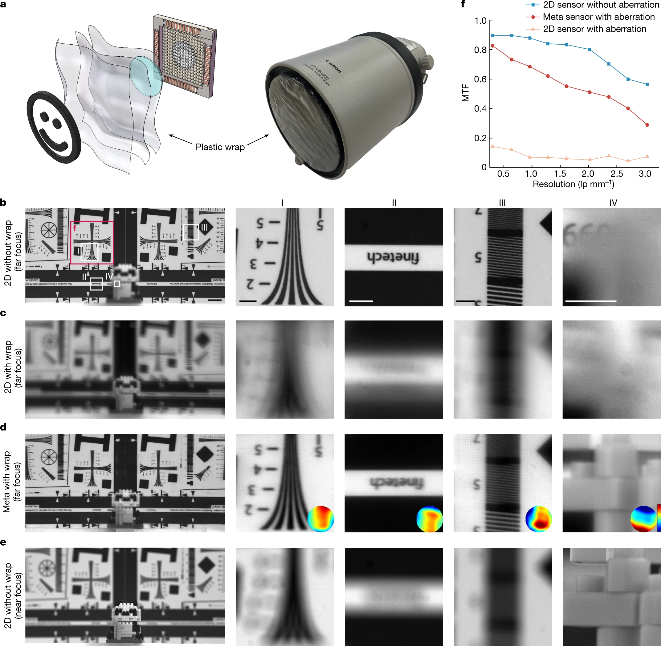
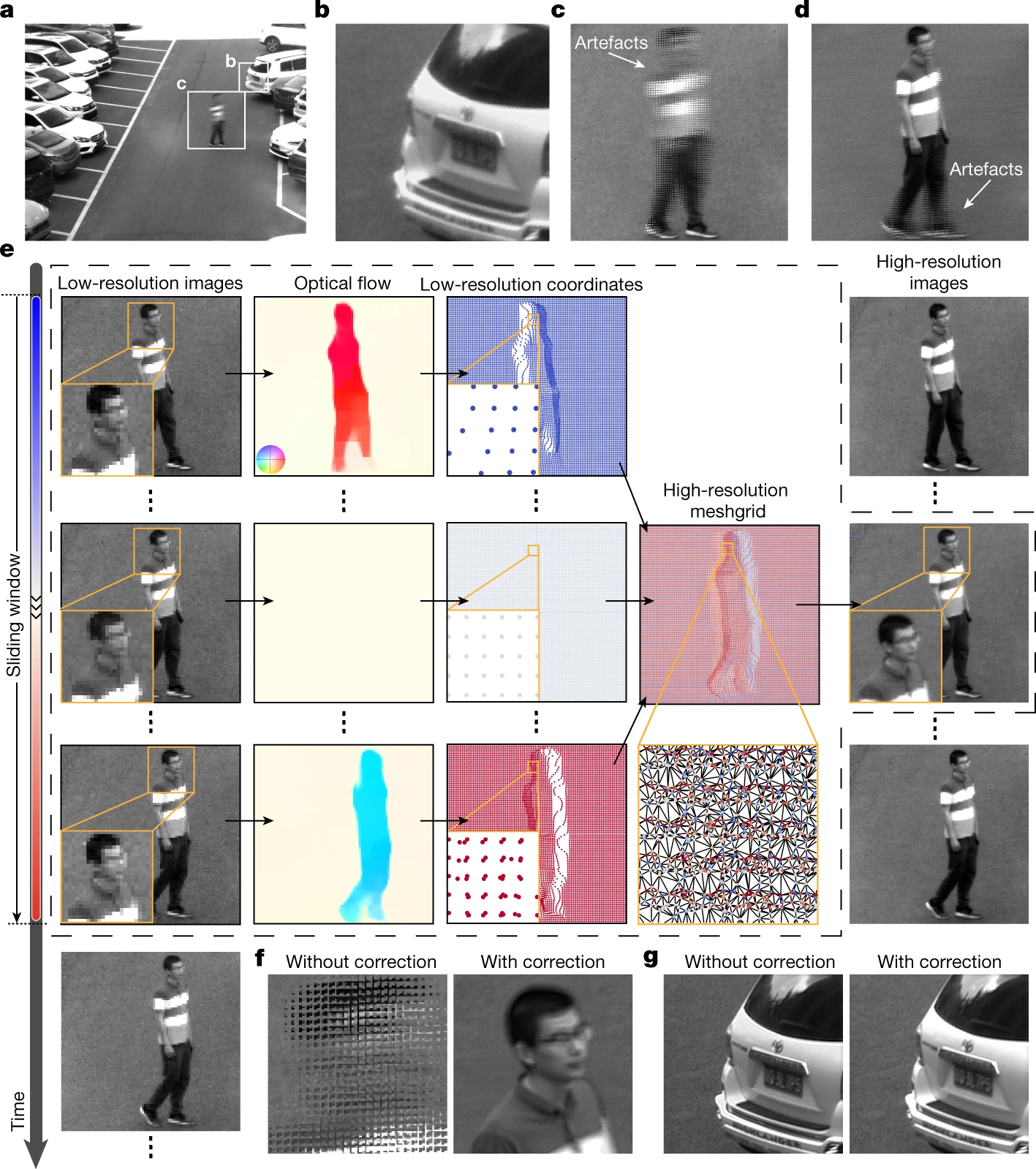
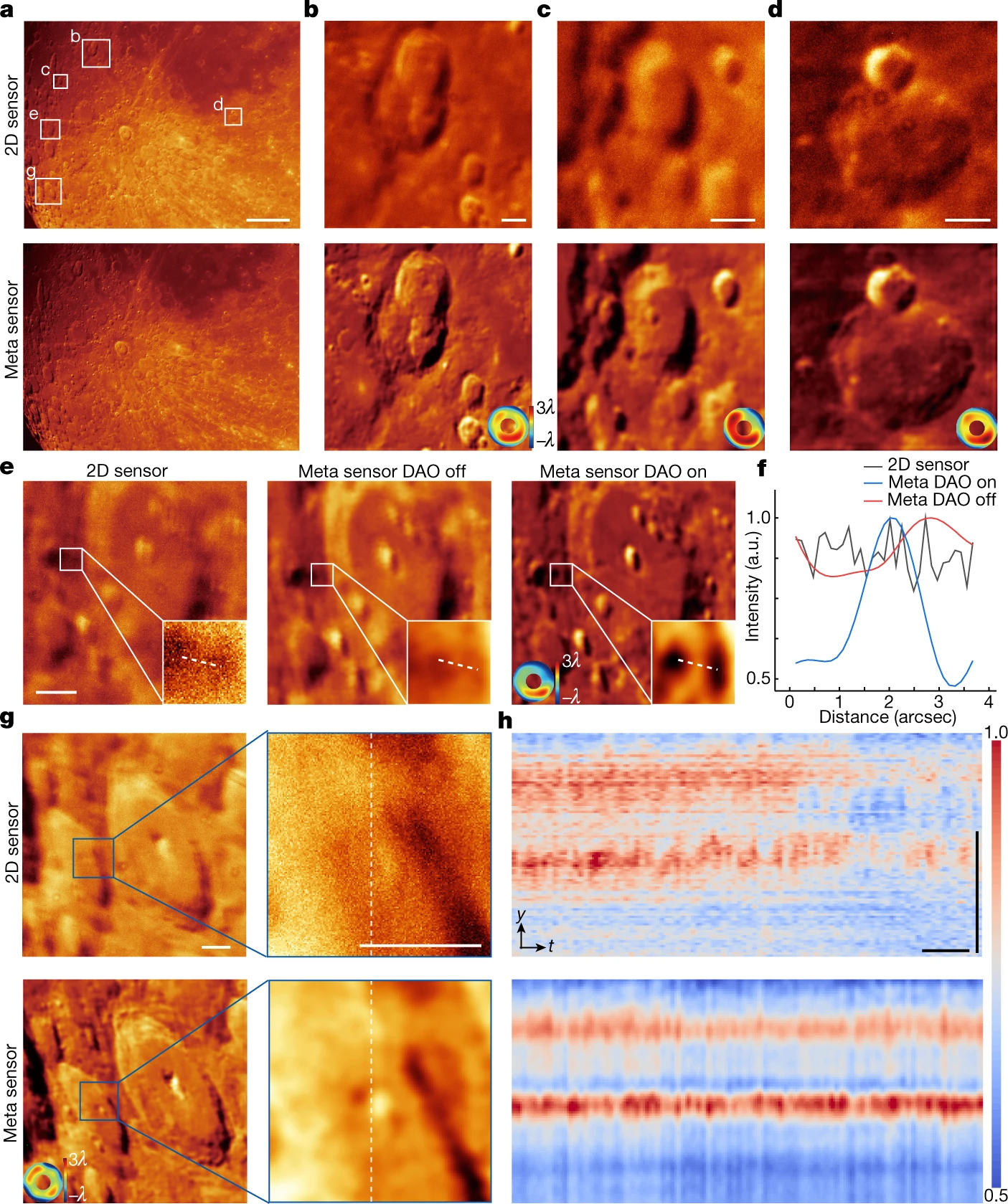
Nature paper on an aberration correcting "meta-image" sensor

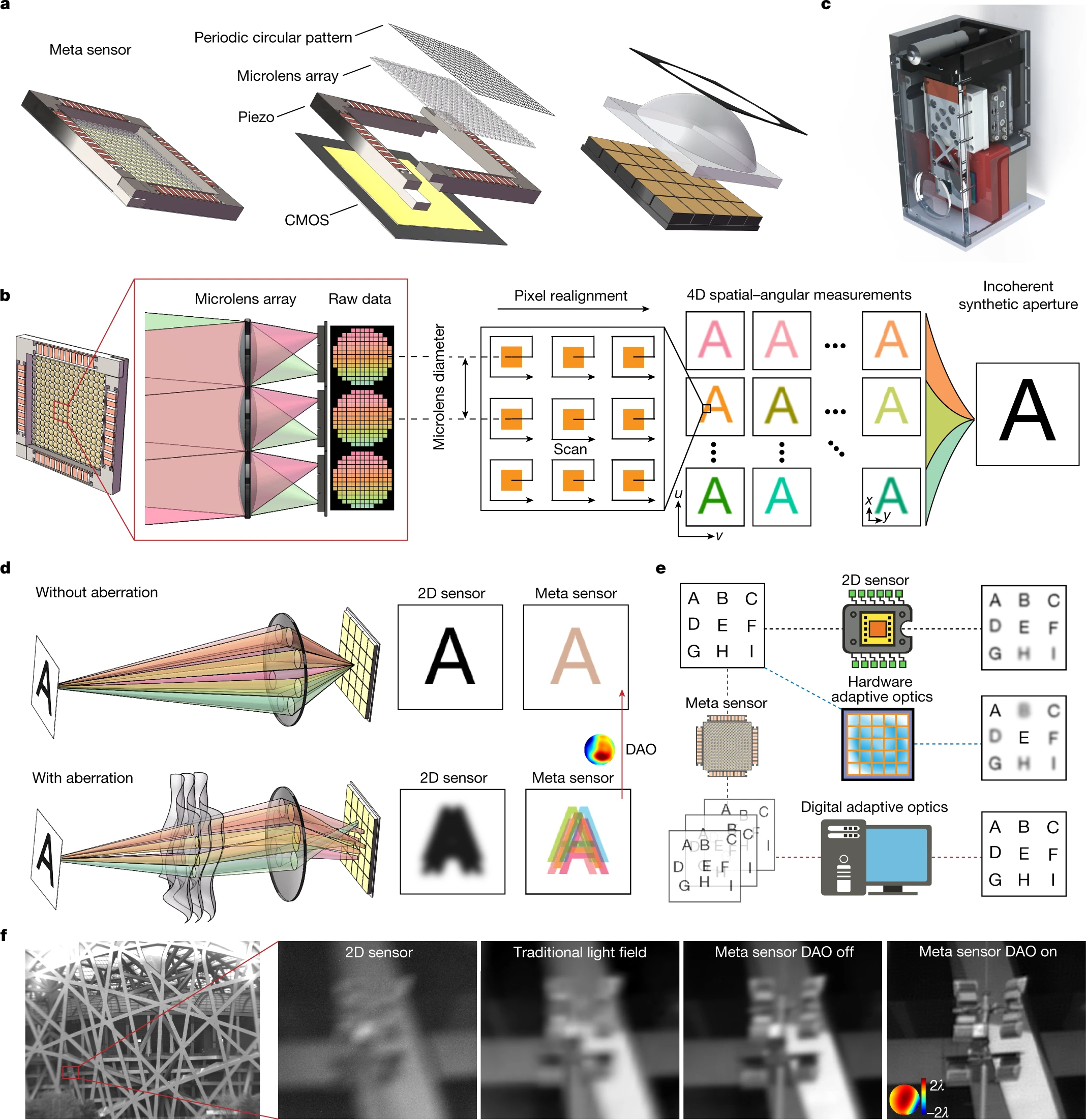
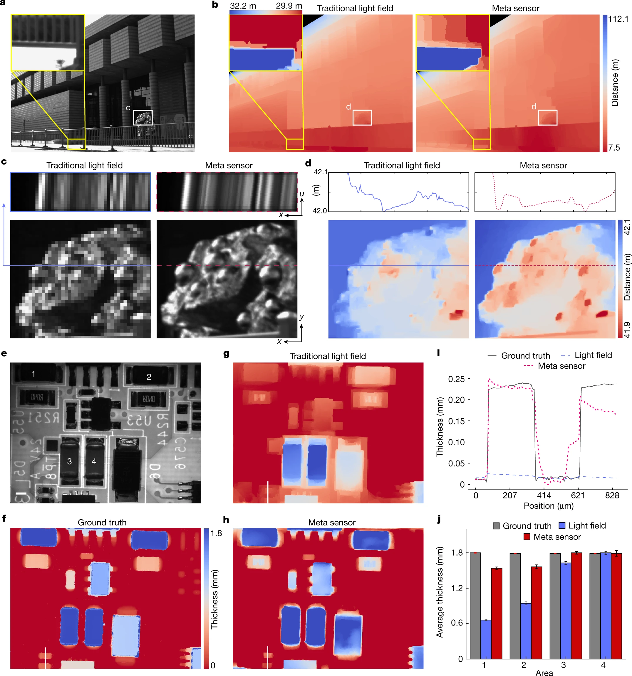
A new paper in Nature titled "An integrated imaging sensor for aberration-corrected 3D photography" by Wu et al. from Tsinghua University presents a new meta-optics based aberration correcting image sensor. They also show several applications such as optical flow and depth imaging in addition to atmospheric aberration correction.

The full paper is open access: https://www.nature.com/articles/s41586-022-05306-8

Abstract: Planar digital image sensors facilitate broad applications in a wide range of areas and the number of pixels has scaled up rapidly in recent years. However, the practical performance of imaging systems is fundamentally limited by spatially nonuniform optical aberrations originating from imperfect lenses or environmental disturbances. Here we propose an integrated scanning light-field imaging sensor, termed a meta-imaging sensor, to achieve high-speed aberration-corrected three-dimensional photography for universal applications without additional hardware modifications. Instead of directly detecting a two-dimensional intensity projection, the meta-imaging sensor captures extra-fine four-dimensional light-field distributions through a vibrating coded microlens array, enabling flexible and precise synthesis of complex-field-modulated images in post-processing. Using the sensor, we achieve high-performance photography up to a gigapixel with a single spherical lens without a data prior, leading to orders-of-magnitude reductions in system capacity and costs for optical imaging. Even in the presence of dynamic atmosphere turbulence, the meta-imaging sensor enables multisite aberration correction across 1,000 arcseconds on an 80-centimetre ground-based telescope without reducing the acquisition speed, paving the way for high-resolution synoptic sky surveys. Moreover, high-density accurate depth maps can be retrieved simultaneously, facilitating diverse applications from autonomous driving to industrial inspections.


Wednesday, November 09, 2022

Yole publishes a market report for X-ray detectors

https://www.yolegroup.com/product/report/x-ray-imaging/


Market dynamics in digital X-ray imaging have been impacted by the Covid crisis, the current geopolitical context and new environmental policies. The Covid crisis upset demand in medical systems in 2020 and 2021. Healthcare facilities prioritized their budgets to fight Covid, boosting static radiography and computed tomography (CT). Many surgeries, mammographies or dental diagnoses have been delayed, slowing demand in these segments by about a year. The medical business eventually returned to its pre-Covid dynamic and is expected to grow from $1,780M in 2021 to $2,128M in 2027 at the detector level. The security business suffered in 2020 and 2021, with airport shutdowns and borders closing. But now the recovery of air transportation and the tense geopolitical context with the Ukraine-Russia war is driving demand in this segment. Security is expected to go from $50M in 2021 to $57M in 2027. Industry also suffered from a global economic downturn due to Covid. However, car electrification is now a good driver for X-ray inspection, which is used in electronics and battery production lines and storage to detect defects. As a result, the segment will grow from $210M in 2021 to $263M in 2027.


 Key Features

  •  Market data on key X-ray detector technologies including flat panel aSi, aSe, IGZO or CMOS, CT detectors and linear sensors over medical, industry, security, and veterinary markets. Historical data are displayed from 2018 to 2021 before forecasting the market up to 2027
  •  Comprehensive analysis of the market trends in the different market segments
  •  Understanding of how health and political crises affect the X-ray imaging market
  •  Market share for flat panel detectors, in value
  •  Comprehensive description of the supply chain from system integrators to semiconductor fabs. Highlights of the main changes since the last update of the report
  •  Comprehensive description of technologies including roadmap on photon-counting technology. Analysis of the penetration of IGZO in flat panels

What's new

  •  The covid crisis upset demand in 2020/2021. Combined with conflicts and trade wars, it forced many players to build new supply chains
  •  Commercialization of the first photon-counting CT scanner by Siemens Healthineers
  •  The biggest CT scan system makers made acquisitions to ensure internal capacity of manufacturing photon-counting detectors
  •  Car electrification is pulling demand for X-ray inspection in electronics and battery production lines

Product objectives

  •  Provide an overview of the digital X-ray imaging industry with a focus on detector components including the different types technologies
  •  Provide an understanding of the main trends in the different segments of digital X-ray imaging with forecast on the market value and associated shipment volumes
  •  Give supply chain insights describing the different levels of integration and the players composing the ecosystem. Providing data of market share for the different types of X-ray detectors
  •  Offering technology understanding about the main innovations with associated challenges and roadmaps

Tuesday, November 08, 2022

Ouster and Velodyne Merger

In recent news on consolidation in the LiDAR market, Ouster and Velodyne have announced a merger deal.

Ouster makes "digital" LiDAR sensors based on single photon avalanche diode technology whereas Velodyne is known for their more "traditional" avalanche photodiode based spinning LiDARs.

https://investors.ouster.com/news/news-details/2022/Ouster-and-Velodyne-Announce-Proposed-Merger-of-Equals-to-Accelerate-Lidar-Adoption/default.aspx


SAN FRANCISCO--(BUSINESS WIRE)-- Ouster (NYSE: OUST), a leading provider of high-resolution digital lidar, and Velodyne (NASDAQ: VLDR, VLDRW), a leading global player in lidar sensors and solutions, announced that they have entered into a definitive agreement to merge in an all-stock transaction. The proposed merger is expected to drive significant value creation and result in a strong financial position through robust product offerings, increased operational efficiencies, ​​and a complementary customer base in fast-growing end-markets. Ouster and Velodyne will host a joint webcast on November 7, 2022 at 8:30 AM ET to discuss the planned merger.

Key Strengths of the Combined Company:

  • Operational synergies across engineering, manufacturing, and general administration support an optimized cost-structure
  • Robust product offerings, including verticalized software, to serve a broad set of customers
  • Complementary customer base, partners, and distribution channels, coupled with reduced product costs and an innovative roadmap, to accelerate lidar adoption across fast-growing end markets
  • Extensive intellectual property portfolio with 173 granted and 504 pending patents, backed by over 20 years of combined experience in lidar technology innovation
  • World-class leadership team to be led by Dr. Ted Tewksbury as Executive Chairman of the Board and Angus Pacala as Chief Executive Officer
  • Strong financial position with combined cash balance1 of approximately $355 million as of September 30, 2022
  • Compared to stand-alone cost structures as of September 30, 2022, annualized operating expenditure synergies of at least $75 million expected to be realized within 9 months after transaction-close

 “Ouster’s cutting-edge digital lidar technology, evidenced by strong unit economics and the performance gains of our new products, complemented by Velodyne’s decades of innovation, high-performance hardware and software solutions, and established global customer footprint, positions the combined company to accelerate the adoption of lidar technology across fast-growing markets with a diverse set of customer needs,” said Ouster CEO Angus Pacala. “Together, we will aim to deliver the performance customers demand while achieving price points low enough to promote mass adoption.”
 

“Lidar is a valuable enabling technology for autonomy, with the ability to dramatically improve the efficiency, productivity, safety, and sustainability of a world in motion. We aim to create a vibrant and healthy lidar industry by offering both affordable, high-performance sensors to drive mass adoption across a wide variety of customer applications, and by creating scale to drive profitable and sustainable revenue growth,” said Velodyne CEO Dr. Ted Tewksbury. “The combination of Ouster and Velodyne is expected to unlock enormous synergies, creating a company with the scale and resources to deliver stronger solutions for customers and society, while accelerating time to profitability and enhancing value for shareholders.”


The combined company will offer a robust suite of products to continue to serve a diverse set of end-markets and customers while executing on an innovative product roadmap to meet the future needs of the market. A unified engineering team, compelling product roadmap, and focused customer success team will aim to provide best-in-class support to customers to deliver affordable and more performant sensors. Further, management plans to streamline operating expenditures to build an overall cost structure that is in line with the projected revenue growth of the combined company. ​​Ouster and Velodyne had a combined cash balance of approximately $355 million as of September 30, 2022, and aim to realize annualized cost savings of at least $75 million within 9 months after closing the proposed merger. With an expanded global commercial footprint and distribution network, the combined company expects to deliver increased volumes, reduce product costs, and drive sustainable growth.


Leadership and Governance
The combined company will be led by Angus Pacala, who will serve as Chief Executive Officer, and Dr. Ted Tewksbury, who will serve as Executive Chairman of the Board. The Board will be comprised of eight members, with each company appointing an equal number of members. The full Board and executive team will be announced at a later date.
 

Transaction Details
The merger agreement was signed on November 4, 2022. Under the terms of the agreement, each Velodyne share will be exchanged for 0.8204 shares of Ouster at closing. The transaction will result in existing Velodyne and Ouster shareholders each owning approximately 50% of the combined company, based on current shares outstanding.


The merger transactions are subject to customary closing conditions including shareholder approval by both companies. Both companies will continue to operate their businesses independently until the close of the merger transactions. The merger transactions are expected to be completed in the first half of 2023.


Barclays is serving as financial advisor and Latham & Watkins LLP is serving as legal advisor to Ouster. BofA Securities, Inc. is serving as financial advisor and Skadden, Arps, Slate, Meagher & Flom LLP is serving as legal advisor to Velodyne.


Ouster and Velodyne will each file the full text of the merger agreement with the Securities and Exchange Commission with a Form 8-K within four business days of the date of this release. Investors and security holders of each company are advised to review these filings for the full terms of the proposed combination, as well as any future filings made by the companies, including the Form S-4 Registration Statement to be filed by Ouster and related Joint Proxy Statement/Prospectus included therein. See below under “Additional Information and Where to Find It”.
 

Joint Webcast Information
Ouster and Velodyne will host a joint webcast on November 7, 2022 at 8:30 AM ET to discuss the proposed merger.
Investors and analysts can register for the webcast by visiting the following website: https://event.on24.com/wcc/r/4007460/9C27A5975C89846F7B386331F4D80C90. The webcast will be available as a replay for one year on Ouster’s investor website at https://investors.ouster.com and on Velodyne’s investor website at https://investors.velodynelidar.com.

Monday, November 07, 2022

Edge Impulse and ConservationX Labs Camera for Ecology and Conservation

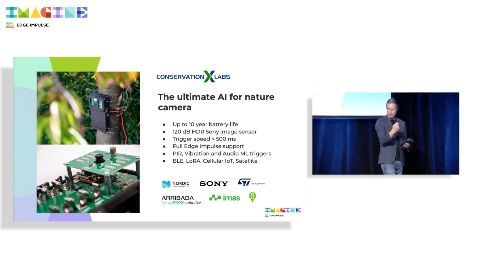
Edge Impulse and Conservation X Labs are teaming up to bring an AI-enabled camera for ecology and wildlife monitoring applications.


https://twitter.com/conservationx/status/1575166560922374144?s=20&t=Nk5lOX69MhcpALGRcMMyHg


Conservation X Labs currently offers a solution called "Sentinel" for AI-on-the-edge using field-deployed cameras and microphones. https://sentinel.conservationxlabs.com/ 

Friday, November 04, 2022

Pixelplus automotive CMOS image sensor

From THEELEC news: https://www.thelec.net/news/articleView.html?idxno=4249

South Korean fabless chip firm Pixelplus will show of engineering samples of its automotive CMOS image sensor to customers during the first quarter.

The new product, called PK5130KA, will begin mass production during the second half of 2023 and contribute to the company’s revenue in 2024, Pixelplus said.

It will the company’s first chip that will be supplied directly to tier-1 suppliers of automobile firms.

Pixelplus had previously supplied such chips through automotive solution firms at a lower price.

Supplying directly to tier-1 suppliers __ called before-market in the industry __ is more difficult due to the harder requirements that they must meet.

Tier-1 suppliers require such chips to meet AEC-Q100 and ISO26262 standards, the global reliability and safety standards.

ISO has ratings from A to D with D being the highest standard. Image sensors require the B grade.

PK5120KA meets these standards, according to Pixelplus. The company is planning to receive the ISO26262 certificate next year.

Pixelplus believes it has a market share of around 5% as of last year in the automotive CMOS image sensor sector.

ONSemiconductor, Sony and Omnivision are the leaders in the market. 

Wednesday, November 02, 2022

Ge-on-Si Image Sensor with NIR Sensitivity

In a recent preprint (https://arxiv.org/ftp/arxiv/papers/2209/2209.14242.pdf) Ponizovskaya-Devine et al. describe a new Ge-on-Si image sensor with enhanced sensitivity up to 1.7um for NIR applications.


Abstract

We present a Germanium “Ge-on-Si” CMOS image sensor with backside illumination for the near-infrared (NIR) electromagnetic waves (wavelength range 300–1700 nm) detection essential for optical sensor technology. The micro-holes help to enhance the optical efficiency and extend the range to the 1.7 µm wavelength. We demonstrate an optimization for the width and depth of the nano-holes for maximal absorption in the near infrared. We show a reduction in the cross-talk by employing thin SiO2 deep trench isolation in between the pixels. Finally, we show a 26–50% reduction in the device capacitance with the introduction of a hole. Such CMOS-compatible Ge-onSi sensors will enable high-density, ultra-fast and efficient NIR imaging.