Business Wire: Global Optics Limited ("Global Optics"), has developed a 1/4" 1.3MP CMOS camera module (CCM) incorporating the "voice coil motor" automatic focus function.
Global Optics was able to enhance the CCM's focus range from 10 centimeters to infinity and improve its response time to about 0.7 seconds.
The most interesting portion of the announcement is "improved image stabilization for taking still pictures".
Wednesday, August 30, 2006
Friday, August 18, 2006
Pixelplus New Pixel
Yahoo-Finance: Pixelplus launches new 1/4.2" PlusPixel(TM) 1.3 Megapixel 'System-On-A-Chip' image sensor with its new foundry partner (probably UMC). Based on 0.13 um CMOS process, the PO5130 uses 2.6um pixel array. This is quite an innefective use of 0.13um process, as most of other companies make 2.2um pixel in this process.
Monday, August 14, 2006
Eamex Image Stabilizer Actuator
Tech-On: Eamex Corp. has developed an actuator for use in optical image stabilizers targeting phonecam modules. Compared to the previous electromagnetic actuators, it boasts a thinner profile as well as simpler structure, lower cost and reduced power consumption.
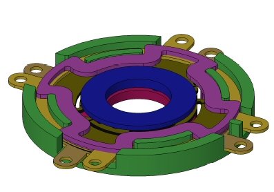
The prototype is as thin as 1.5 mm and measures 14 mm in diameter. The ion exchange resin that supports the lens holder expands and contracts to tilt the lens.
The maximum tilt angle and speed are ±2.9° and 14.13° per second, respectively. The power consumption is 15-35 mW. The drive voltage is ±4 V.
On the picture below a lens holder is disposed in the center:

Thursday, August 10, 2006
TSMC to Increase Its VisEra Investment
EETimes: TSMC's board also approved an increase of the investment not exceeding $27 million in VisEra Technologies (Hsinchu), a provider of CMOS image sensor foundry services.
In October 2003, TSMC and CMOS image sensor maker OmniVision Inc. (Sunnyvale, Calif.) entered into an agreement to form a joint venture called VisEra Technologies in Taiwan. VisEra's mission is to provide manufacturing services and automated final testing in the CMOS image sensor arena.
TSMC and OmniVision also entered into separate non-exclusive license agreements with VisEra pursuant to which each party licenses certain intellectual property to VisEra.
In August 2005, TSMC and OmniVision amended the deal. Under the plan, the parties agreed to raise the total capital committed to the joint venture from $50 million to $68 million.
"The $18.0 million increase was designated principally for the acquisition from existing shareholders of approximately 29.6 percent of the issued share capital of XinTec Inc., or XinTec, a Taiwan-based provider of chip-scale packaging services of which [OmniVision] directly own approximately 7.8 percent," according to a filing by the U.S. supplier of CMOS image sensors.
In fiscal 2006, VisEra invested an additional $0.5 million in XinTec as their portion of an additional capital injection to enable XinTec to expand its production capacity.
In total, TSMC and OmniVision increased their stake in VisEra from 25 percent to 43 percent. In the quarter ended January 2006, the two companies increased its interest in VisEra from 43 percent to 46 percent through purchases of unissued shares.
In January 2006, VisEra purchased from TSMC the equipment used for applying color filers and micro-lenses to wafers. VisEra is now providing the related processing services that OmniVision previously purchased from TSMC.
"We outsource our wafer manufacturing for CameraChip image sensors to Taiwan Semiconductor Manufacturing Company, or TSMC, and Powerchip Semiconductor Corp., or PSC," according to OmniVision in a recent filing. "In addition, TSMC and Semiconductor Manufacturing International Corporation, or SMIC, fabricate our companion DSP chips."
ESS Transcripts Funny Mistakes
ESS Q4'05 conference call transcript has a funny mistake in it:
"Now I’ll give you an update on our camera phone business. Our Digital Imaging business had revenues of approximately $5.4 million in the fourth quarter inline with our estimates. These revenues came primarily from shipments of 1.3 Megapixel launches for Samsung and 1.3 mega pixel chips sales to LG Electronics. We continue to move our business model away from selling modules to selling silicon chips only. Our major customers are inline with this strategy and we were working with several margin manufacturers worldwide.
Today we have camera designs in many different handsets worldwide. Many of these new designs come from Korea both from Samsung and LG as we mentioned previously towards all kind of manufactures in the world. We also planned an additional higher performance lower cost integrated image sensor and image processor systems on a chips in the next several months. These chips will utilize advance 40 and shared 40 pixel technologies. We demonstrated a new 41.3 Megapixel system on chip at the CES show this year and we will sample this product this month.
The initial feedback from our customers with the quality of the pictures taken with this chip is very nice, is very good and we believe it will be well received by the market. We believe these new products puts forth the base for future growth for the camera phone business. And I will get detailed guidance for ESS business in the first quarter of 2006."
Now what is 41.3 Megapixel? It was supposed to be "four-tee one point three megapixel = 4T 1.3MP", I believe. Same manner, "40 pixel technologies" are probably "4T pixel technologies".
In Q1'06 conference call transcript there is a similar mistake:
"Now, I'll give you an update on our camera phone business. Our digital imaging business had revenues of approximately $2.5 million in the first quarter inline with our estimates. These revenues came primarily from shipments of our 1.3 megapixel chips to LG Electronics.
Today, we are currently sampling our new 4T 1.3 megapixel, system-on-chip to customers worldwide. We are also developing new higher-performance, lower-cost, integrated image sensor and image process system-on-a-chip, which we plan to introduce to the market later this year. These new chips will utilize events, share at 14 pixel technologies, and we believe these advanced 4T-shared products will provide ESS with the combination of high-performance and low-cost products that the camera phone market requires."
14 shared pixel probably comes from they are saying "shared four-tee pixel=4T pixel" which sounds like "share at 14 pixel"
Wednesday, August 09, 2006
Photobit History
CBR Center of Oxford University published a few bits of Photobit history:
Photobit was founded by Dr Eric Fossum and associates from NASA s Jet Propulsion Laboratory in 1995 to commercialise the CMOS image sensor technology he had invented there as manager of its image sensor and focal plane R&D programmes. He has over 90 US patents. Photobit used an SBIR contract from the US Army Development Test Command to develop high-resolution, high-speed, low-power image sensors for recording the details of missile launches on test ranges. This initial work led to the development of megapixel Complementary Metal Oxide Semiconductor (CMOS) image sensors with speeds greater than 500 frames per second and electronic shuttering capability that could freeze even the fastest motion to create high quality images. Photobit also used an SBIR award from DARPA to develop a micro-sized, micropower CMOS sensor: its small size and very low power enabled the development of the swallowable pill-camera that is now gaining widespread acceptance for noninvasive medical imaging of the gastrointestinal system.
The company also won SBIR contracts from NASA and the Ballistic Missile Defence Organisation (now MDA),and the Navy also used Photobit s technology to build airborne weapon separation monitoring cameras. Though Photobit s early development was largely funded from government contracts, its technology became increasingly used in a range of commercial applications. These included industrial machine vision, high-speed industrial/scientific imaging, biomechanics, and animation systems for motion pictures, television and video games. Cameras using its technology captured various industry awards and were used in films such as The Mummy II and Star Wars Episode II . As the technology improved and manufacturing costs fell, there were also increasing opportunities for volume applications in digital cameras and mobile phones.
By 2000 Photobit had annual revenues of $20m, and on the back of the further significant growth potential from consumer applications the company was able to attract a $26m venture capital investment from Intel, Hitachi and Basler A.G. In 2001, Micron Technology Inc, a $4 billion revenue semiconductor company based in Boise, Idaho, acquired the business in an effort to enter this fast growing market. It did not announce the acquisition for 6 months, an indication of the strategic significance of the move to the corporation. By this time it had integrated Photobit's operations and put in place aggressive plans to grow the business, which it renamed Micron Imaging. As Shawn Maloney, Senior Director of Marketing at Micron Imaging put it, "Micron does not enter markets it doesn t plan to dominate." Micron is now the world s leading supplier of CMOS image sensors.
Dr Fossum has now moved on to another young,growing high-technology company,Siimpel,which is using MEMS technology to develop a high-quality cost-effective optical solution for camera phones. This work has also been supported by various SBIR and other federal government R&D programmes. Dr Fossum says, "I am a strong advocate of the US SBIR programme as I think there need to be channels other than traditional venture capital to seed new technology businesses. SBIR awards help companies that wouldn t otherwise attract venture capital funding because they have a slow growth profile,or a niche market appeal."
"They help entrepreneurs because they allow more self-start and less dilution for the founders of such companies. But they are also very helpful to the government on many levels,seeding businesses that are developing technologies useful to government agencies and,often, to us all. "
Tuesday, August 08, 2006
Lyra Research on Camera Phones
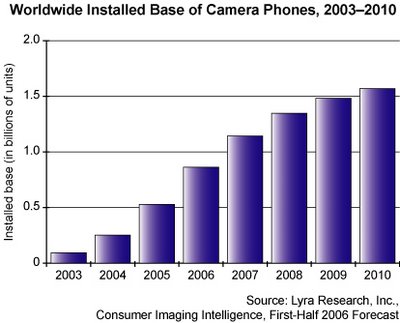
PRWeb: Lyra estimates that the installed base of camera phones will reach approximately 850 million units in 2006, and this number is expected to grow to more than 1.5 billion units in 2010 (see figure).


Monday, August 07, 2006
Atmel Sold Its Image Sensor Business to e2v
EETimes: Atmel Corp. signed an agreement to sell its Grenoble, France subsidiary and the wafer fab to e2v technologies plc (Chelmsford, U.K.) for approximately $140 million in cash. Most of Grenoble products, including image sensors and aerospace qualified microprocessors, will be part of the sale.
Sunday, August 06, 2006
Planet82 Adds Color Capability
Planet82 announced "Color Nano Image Sensor". The high sensitive color nano image sensor is upgrade version of the black and white sensor which had announced in Korea in November 2005.
The company completed product development for mass production sensor for surveillance system. This Color Nano Image Sensor allows capturing 30 frames color moving pictures under 0.1lux and is able to shoot 100 frames under regular illumination conditions.
In another note Planet82 announces "500 times superior sensitivity specification compare to existing CCD and CMOS with 1/2 size".
In yet another note the company announced a 3-year agreement with IBM to use IBM as a foundry to mass produce its sensors.
Saturday, August 05, 2006
Micron Revealed Osmium Packaging Technology
EETimes: Micron revealed a new packaging technology that can be applied to reduce the footprint of both semiconductor devices and image sensors.
"Osmium" package is still in development but has the potential to half die size by eliminating wire bonds completely. In the through-wafer interconnects (TWI) technique holes are drilled directly through the die bond pad and a conductive material fills them. This provides the shortest route for a connection to the bond of a second die. Using redistributed layer technology allows for pad balls to be redistributed from the die bond to meet standard and custom ball patterns at the edge of the die. Finally the wafer-level encapsulation encloses the die on all six sides while it is still part of the wafer.
The packaged parts are mere microns larger than a bare die device at a lower cost, since batch processing die can increase manufacturing efficiency.
The side benefit to Micron is that its memory devices and image sensors potentially can be made without leadframes and substrates and reduce the packaging cost, now estimated to comprise 15 to 25 percent of the finished product cost.
Wednesday, August 02, 2006
Canon HDTV Image Sensor
Yahoo-Finance: Canon launched consumer HDV camcorder with its own CMOS sensor. The 1/2.7" sensor incorporates an RGB primary color filter with Bayer placement. This sensor supplies 1080 HD video to an HDV video tape, while 3.1 megapixel still images.
CamcorderInfo.com adds few more details: The sensor resolution is 2.96 gross MP, 2.07 effective MP. The sensor "offers noise reduction built into the chip".
CamcorderInfo.com adds few more details: The sensor resolution is 2.96 gross MP, 2.07 effective MP. The sensor "offers noise reduction built into the chip".
Subscribe to:
Posts (Atom)