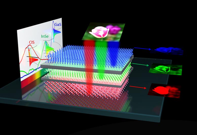
“This work is the first step toward our final destination–to develop a micro-scale camera for microrobots,” says assistant professor of Physics Sidong Lei, who led the research. “We illustrate the fundamental principle and feasibility to construct this new type of image sensor with emphasis on miniaturization.”
Friday, April 29, 2022
Color sensing for nano-vision-sensors
Thursday, April 28, 2022
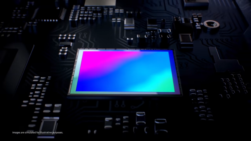
Samsung making a new larger ISOCELL camera sensor?
Wednesday, April 27, 2022
90-min Tutorial on Single Photon Detectors
Tuesday, April 26, 2022
Embedded Vision Summit 2022
- Keynote speaker Prof. Ryad Benosman of University of Pittsburgh and the CMU Robotics Institute will speak on “Event-based Neuromorphic Perception and Computation: The Future of Sensing and AI”
- General session speakers include:
- Zach Shelby, co-founder and CEO of Edge Impulse, speaking on “How Do We Enable Edge ML Everywhere? Data, Reliability, and Silicon Flexibility”
- Ziad Asghar, Vice President of Product Management at Qualcomm, speaking on “Powering the Connected Intelligent Edge and the Future of On-Device AI”
- 90+ sessions across four tracks—Fundamentals, Technical Insights, Business Insights, and Enabling Technologies
- 60+ exhibitors including Premier Sponsors Edge Impulse and Qualcomm, Platinum Sponsors FlexLogix and Intel, and Gold Sponsors Arm, Arrow, Avnet, BDTi, City of Oulu, Cadence, Hailo, Lattice, Luxonis, Network Optics, Nota, Perceive, STMicroelectronics, Synaptics and AMD Xilinx
- Deep Dive Sessions — offering opportunities to explore cutting-edge topics in-depth — presented by Edge Impulse, Qualcomm, Intel, and Synopsys
- “We are delighted to return to being in-person for the Embedded Vision Summit after two years of online Summits,” said Jeff Bier, founder of the Edge AI and Vision Alliance. “Innovation in visual and edge AI continues at an astonishing pace, so it’s more important than ever to be able to see, in one place, the myriad of practical applications, use cases and building-block technologies. Attendees with diverse technical and business backgrounds tell us this is the one event where they get a complete picture and can rapidly sort out the hype from what’s working. A whopping 98% of attendees would recommend attending to a colleague.”
Half a billion years ago something remarkable occurred: an astonishing, sudden increase in new species of organisms. Paleontologists call it the Cambrian Explosion, and many of the animals on the planet today trace their lineage back to this event.A similar thing is happening in processors for embedded vision and artificial intelligence (AI) today, and nowhere will that be more evident than at the Embedded Vision Summit, which will be an in–person event held in Santa Clara, California, from May 16–19. The Summit focuses on practical know–how for product creators incorporating AI and vision in their products. These products demand AI processors that balance conflicting needs for high performance, low power, and cost sensitivity. The staggering number of embedded AI chips that will be on display at the Summit underscores the industry’s response to this demand. While the sheer number of processors targeting computer vision and ML is overwhelming, there are some natural groupings that make the field easier to comprehend. Here are some themes we’re seeing.
Founded in 2011, the Edge AI and Vision Alliance is a worldwide industry partnership that brings together technology providers who are enabling innovative and practical applications for edge AI and computer vision. Its 100+ Member companies include suppliers of processors, sensors, software and services.First, some processor suppliers are thinking about how to best serve applications that simultaneously apply machine learning (ML) to data from diverse sensor types — for example, audio and video. Synaptics’ Katana low–power processor, for example, fuses inputs from a variety of sensors, including vision, sound, and environmental. Xperi’s talk on smart toys for the future touches on this, as well.Second, a subset of processor suppliers are focused on driving power and cost down to a minimum. This is interesting because it enables new applications. For example, Cadence will be presenting on additions to their Tensilica processor portfolio that enable always–on AI applications. Arm will be presenting low–power vision and ML use cases based on their Cortex–M series of processors. And Qualcomm will be covering tools for creating low–power computer vision apps on their Snapdragon family.Third, although many processor suppliers are focused mainly or exclusively on ML, a few are addressing other kinds of algorithms typically used in conjunction with deep neural networks, such as classical computer vision and image processing. A great example is quadric, whose new q16 processor is claimed to excel at a wide range of algorithms, including both ML and conventional computer vision.Finally, an entirely new species seems to be coming to the fore: neuromorphic processors. Neuromorphic computing refers to approaches that mimic the way the brain processes information. For example, biological vision systems process events in the field of view, as opposed to classical computer vision approaches that typically capture and process all the pixels in a scene at a fixed frame rate that has no relation to the source of the visual information. The Summit’s keynote talk, “Event–based Neuromorphic Perception and Computation: The Future of Sensing and AI” by Prof. Ryad Benosman, will give an overview of the advantages to be gained by neuromorphic approaches. Opteran will be presenting on their neuromorphic processing approach to enable vastly improved vision and autonomy, the design of which was inspired by insect brains.Whatever your application is, and whatever your requirements are, somewhere out there is an embedded AI or vision processor that’s the best fit for you. At the Summit, you’ll be able to learn about many of them, and speak with the innovative companies developing them. Come check them out, and be sure to check back in 10 years — when we will see how many of 2032’s AI processors trace their lineage to this modern–day Cambrian Explosion!—Jeff Bier is the president of consulting firm BDTI, founder of the Edge AI and Vision Alliance, and the general chair of the Embedded Vision Summit.
- Inspiring and empowering product creators to incorporate AI and vision technology into new products and applications
- Helping Member companies achieve success with edge AI and vision technology by:
- Building a vibrant AI and vision ecosystem by bringing together suppliers, end-product designers, and partners
- Delivering timely insights into AI and vision market research, technology trends, standards and application requirements
- Assisting in understanding and overcoming the challenges of incorporating AI in their products and businesses
Monday, April 25, 2022
Perspective article on solar-blind UV photodetectors
Friday, April 22, 2022
Videos du jour - CICC, PhotonicsNXT and EPIC
IEEE CICC 2022 best paper candidates present their work
PhotonicsNXT Fall Summit keynote discusses automotive lidar
This keynote session by Pierrick Boulay of Yole Developpement at the PhotonicsNXT Fall Summit held on October 28, 2021 provides an overview of the lidar ecosystem and shows how lidar is being used within the auto industry for ranging and imaging.
EPIC Online Technology Meeting on Single Photon Sources and Detectors
The power hidden in one single photon is unprecedented. But we need to find ways to harness that power. This meeting will discuss cutting-edge technologies paving the way for versatile and efficient pure single-photon sources and detection schemes with low dark count rates, high saturation levels, and high detection efficiencies. This meeting will gather the key players in the photonic industry pushing the development of these technologies towards commercializing products that harness the intrinsic properties of photons.
Thursday, April 21, 2022
Wide field-of-view imaging with a metalens
Wide-angle imaging is an important function in photography and projection, but it also places high demands on the design of the imaging components of a camera. To eliminate the coma caused by the focusing of large-angle incident light, traditional wide-angle camera lenses are composed of complex optical components. Here, we propose a planar camera for wide-angle imaging with a silicon nitride metalens array mounted on a CMOS image sensor. By carefully designing proper phase profiles for metalenses with intentionally introduced shifted phase terms, the whole lens array is capable of capturing a scene with a large viewing angle and negligible distortion or aberrations. After a stitching process, we obtained a large viewing angle image with a range of >120 degrees using a compact planar camera. Our device demonstrates the advantages of metalenses in flexible phase design and compact integration, and the prospects for future imaging technology.
Wednesday, April 20, 2022
PhD Thesis on Analog Signal Processing for CMOS Image Sensors
The very first PhD thesis that came out of Albert Theuwissen's group at TU Delft is now freely available as a pdf. This seems like a great educational resource for people interested in image sensors.
Direct download link: https://repository.tudelft.nl/islandora/object/uuid:2fbc1f51-7784-4bcd-85ab-70fc193c5ce9/datastream/OBJ/download
This thesis describes the development of low-noise power-efficient analog interface circuitry for CMOS image sensors. It focuses on improving two aspects of the interface circuitry: firstly, lowering the noise in the front-end readout circuit, and secondly the realization of more power-efficient analog-to-digital converters (ADCs) that are capable of reading out high-resolution imaging arrays.Chapter 2 provides an overview of the analog signal processing chain in conventional, commercially-available CMOS imagers. First of all, the different photo-sensitive elements that form the input to the analog signal chain are briefly discussed. This is followed by a discussion of the analog signal processing chain itself, which will be divided into two parts. Firstly, the analog front-end, consisting of in-pixel circuitry and column-level circuitry, is discussed. Second, the analog back-end, consisting of variable gain amplification and A/D conversion is discussed. Finally, a brief overview of advanced readout circuit techniques is provided.
In chapter 3, the performance of the analog front-end is analyzed in detail. It is shown that its noise performance is the most important parameter of the front-end. An overview of front-end noise sources is given and their relative importance is discussed. It will be shown that 1/f noise is the limiting noise source in current CMOS imagers. A relatively unknown 1/f noise reduction technique, called switched-biasing or large signal excitation (LSE), is introduced and its applicability to CMOS imagers is explored. Measurement results on this 1/f noise reduction technique are presented. Finally, at the end of the chapter, a preliminary conclusion on CMOS imager noise performance is presented.
The main function of the back-end analog signal chain is analog-to-digital conversion, which is described in chapter 4. First of all, the conventional approach of a single chip-level ADC is compared to a massively-parallel, column-level ADC, and the advantages of the latter will be shown. Next, the existing column-level ADC architectures will be briefly discussed, in particular the column-parallel single-slope ADC. Furthermore, a new architecture, the multiple-ramp single-slope ADC will be proposed. Finally, two circuit techniques are introduced that can improve ADC performance. Firstly, it will be shown that the presence of photon shot noise in an imager can be used to significantly decrease ADC power consumption. Secondly, an column FPN reduction technique, called Dynamic Column Switching (DCS) is introduced.
Chapter 5 and 6 present two realisations of imagers with column-level ADCs. In chapter 5, a CMOS imager with single-slope ADC is presented that consumes only 3.2µW per column. The circuit details of the comparator achieving this low power consumption are described, as well as the digital column circuitry. The ADC uses the dynamic column switching technique introduced in chapter 4 to reduce the perceptional effects of column FPN. Chapter 6 presents an imager with a multiple-ramp single-slope architecture, which was proposed in chapter 4. The column comparator used in this design is taken from a commercially available CMOS imager. The multiple ramps are generated on chip with a low power ladder DAC structure. The ADC uses an auto-calibration scheme to compensate for offset and delay of the ramp drivers.
Tuesday, April 19, 2022
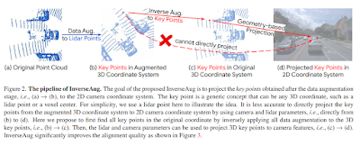
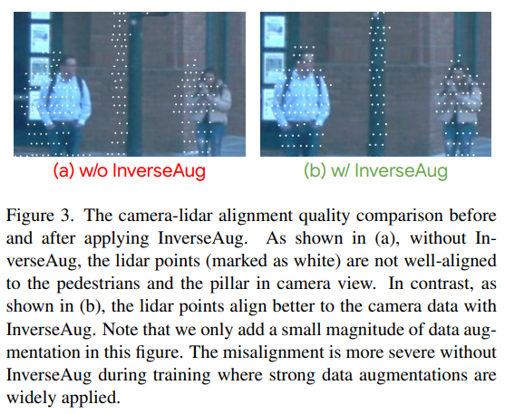
Google AI Blog article on Lidar-Camera Fusion
Monday, April 18, 2022
Quantum Dot Photodiodes for SWIR Cameras
A research team from Ghent University in Belgium has published an article titled "Colloidal III–V Quantum Dot Photodiodes for Short-Wave Infrared Photodetection".
Abstract: Short-wave infrared (SWIR) image sensors based on colloidal quantum dots (QDs) are characterized by low cost, small pixel pitch, and spectral tunability. Adoption of QD-SWIR imagers is, however, hampered by a reliance on restricted elements such as Pb and Hg. Here, QD photodiodes, the central element of a QD image sensor, made from non-restricted In(As,P) QDs that operate at wavelengths up to 1400 nm are demonstrated. Three different In(As,P) QD batches that are made using a scalable, one-size-one-batch reaction and feature a band-edge absorption at 1140, 1270, and 1400 nm are implemented. These QDs are post-processed to obtain In(As,P) nanocolloids stabilized by short-chain ligands, from which semiconducting films of n-In(As,P) are formed through spincoating. For all three sizes, sandwiching such films between p-NiO as the hole transport layer and Nb:TiO2 as the electron transport layer yields In(As,P) QD photodiodes that exhibit best internal quantum efficiencies at the QD band gap of 46±5% and are sensitive for SWIR light up to 1400 nm.
Full article (open access): https://onlinelibrary.wiley.com/doi/10.1002/advs.202200844
Friday, April 15, 2022
PreAct Technologies and ESPROS Photonics Collaborate on Next-Generation Sensing Solutions
PreAct Technologies, an Oregon-based developer of near-field flash LiDAR technology and ESPROS Photonics, a Swiss company leader in the design and production of time-of flight chips and 3D cameras, recently announced a collaboration agreement to develop new flash LiDAR technologies for specific use cases in automotive, trucking, industrial automation and robotics. The collaboration combines the dynamic abilities of PreAct’s software-definable flash LiDAR and the versatile and ultra-ambient-light-robust time-of flight technology from ESPROS to create next-generation near-field sensing solutions.
“Our partnership with ESPROS is a major milestone for our company in our goal to provide high performance, software-definable sensors to meet the needs of customers across various industries,” said Paul Drysch, CEO and co-founder of PreAct Technologies. “Looking to the future, vehicles across all industries will be software-defined, and our flash LiDAR solutions are built to support that infrastructure from the beginning.”
Thursday, April 14, 2022
New Videos from IEEE Sensors Council
Ultra-Thin Image Sensor Chip Embeded Foil
Author: Shuo Wang{2}, Björn Albrecht{1}, Christine Harendt{1}, Jan Dirk Schulze Spüntrup{1}, Joachim Burghartz{1}
Affiliation: {1}Institut für Mikroelektronik Stuttgart, Germany; {2}Institut für Nano- und Mikroelektronische Systeme, Germany
Abstract: Hybrid Systems in Foil (HySiF) is an integration concept for high-performance and large-area flexible electronics. The technology allows for integrating ultra-thin chips and widely distributed electronic components, such as sensors, microcontrollers or antennas, in thin flexible polymer film, using CMOS-compatible equipment and processing. This paper focuses on the embedding and characterization of a bendable ultra-thin image sensor in flexible polymer foil.
Wednesday, April 13, 2022
Harvest Imaging Forum 2022 is open for registration!
After the Harvest Imaging forums during the last 7 years, an eighth one will be organized on June 23 & 24, 2022 in Delft, the Netherlands. The basic intention of the Harvest Imaging forum is to have a scientific and technical in-depth discussion on one particular topic that is of great importance and value to digital imaging. Due to well-known reasons, the 2022 version of the forum will be organized in a hybrid form :
You can attend in-person and can benefit in an utmost way of the live interaction with the speakers and audience,
There will be also a live broadcast of the forum, still interactions with the speakers through a chat box will be made possible,
Finally the forum also can be watched on-line at a later date.
The 2022 Harvest Imaging forum will deal with two subjects in the field of solid-state imaging and two speakers. Both speakers are world-level experts in their own fields.
"Dark current, dim points and bright spots : coming to the dark side of image sensors"
Dr. Daniel McGrath (GOODiX, USA)
Abstract:
Charge-generating defects are an intersection of physics, material properties, manufacturing processes and image science. In this time when pixels are reduced in dimensions comparable to the wavelength of light and noise performance is approaching photon counting, processes that produce erroneous signals in the dark have come to limit image sensor performance. The reduction of dark current over the last decades has been a success story, but has got the industry to a point where it is not clear the path for further improvement.
The aim of this forum is to provide an feet-on-the-ground exploration of the nature of dark current and of bright defects in image sensors. The start will be a discussion of the nature of both with their individual challenges and a timeline to put the development that has got the technology to its present state. It will discuss the challenge and opportunity provided by extreme sensitivity of the pixel, a curse and a blessing for understanding. It will traverse the physics and material issues related in spontaneous charge generation in semiconductors. It will take time to ponder gettering, passivation and radiation effects. It will try to provide a path through the tangle of manufacturing's mysteries and challenges. The goal is to climb to the present precipice, there to consider options that can take the technology to the next advance.
Bio:
Dan McGrath has worked for 40 years specializing in the device physics of silicon-based pixels, CCD and CIS, and in the integration of image-sensor process enhancements in the manufacturing flow. He chose his first job because it offered that “studying defects in image sensors means doing physics” and has kept this passion front-and-center in his work. After obtaining his doctorate from The Johns Hopkins University, he pursued this work at Texas Instruments, Polaroid, Atmel, Eastman Kodak, Aptina and BAE Systems. He has worked with manufacturing facilities in France, Italy, Taiwan, and the USA. In 2019 he joined GOODiX Technology, a supplier to the cell phone and IoT market. He has held organizational positions in the Semiconductor Interface Specialists Conference, the International Solid State Circuits Conference, The International Electron Device Conference and the International Image Sensor Workshop. He has made presentations on dark current at ESSDERC, Electronic Imaging and the International Image Sensor Workshop. His publications include the first megapixel CCD and the basis for dark current spectroscopy (DCS).
"Random Telegraph Signal and Radiation Induced Defects in CMOS Image Sensors"
Dr. Vincent Goiffon (ISAE-SUPAERO, Fr)
Abstract:
CMOS Image Sensors (CIS) are by far the main solid-state image sensor technology in 2021. Each and every year, this technology comes closer to the ideal visible imaging device with near 100% peak quantum efficiency, sub electron readout noise and ultra-low dark current (< 1 e-/s) at room temperature. In such near-perfect pixel arrays, the appearance of a single defect can seriously jeopardize the pixel function. Oxide/silicon interface and silicon bulk defects can remain after manufacturing or can be introduced by aging or after exposure to particle radiation. This later source of performance degradation limits the use of commercial “unhardened” solid-state sensors in a wide range of key applications such as medical imaging, space exploration, nuclear power plant safety, electron microscopy, particle physics and nuclear fusion instrumentation.
The aim of this forum is to explore the influence of semiconductor defects on CIS performances through the magnifying glass of radiation damage. In a first part, a review of radiation effects on CIS will be provided alongside the main mitigation techniques (so-called radiation hardening by design or RHBD techniques). The trade-off between radiation-hardening and performance will be discussed on chosen applications. This first part has a double objective: 1) to provide image sensors professionals the background to anticipate and improve the radiation hardness of their sensors in radiation environment, and 2) to give a different perspective on parasitic physical mechanisms that can be observed in as-fabricated sensors such as hot pixels and charge transfer inefficiency.
The second part will focus on Random Telegraph Signals (RTS) in image sensors, a defect related phenomenon of growing importance in advanced technologies. The fundamental differences between the two main RTS in imagers – MOSFET channel RTS, also called RTN, and Dark Current RTS (DC-RTS) – will be presented. Similarly to the first part, radiation damage will be used to clarify the mysterious origin of DC-RTS. The discussion will conclude with an opening towards the RTS mechanisms similarities between CIS and other image sensor technologies (e.g. SPAD and infrared detectors) and integrated circuits (DRAM).
Bio:
Vincent Goiffon received his Ph.D. in EE from the University of Toulouse in 2008. The same year he joined the ISAE-SUPAERO Image Sensor Research group as Associate Professor and he has been a Full Professor of Electronics at the Institute since 2018.
He has contributed to advance the understanding of radiation effects on solid-state image sensors, notably by identifying original degradation mechanisms in pinned photodiode pixels and by clarifying the role of interface and bulk defects in the mysterious dark current random telegraph signal phenomenon.
Besides his contributions to various space R&D projects, Vincent has been leading the development of radiation hardened CMOS image sensors (CIS) and cameras for nuclear fusion experiments (e.g. ITER and CEA Laser MegaJoule) and nuclear power plant safety. Vincent recently became the head of the Image Sensor Group of ISAE-SUPAERO.
Vincent Goiffon is the author of one book chapter and more than 90 scientific publications, including more than 10 conference awards at IEEE NSREC, RADECS and IISW.
He has been an associate editor of the IEEE Transactions on Nuclear Science since 2017 and has served the community as reviewer and session chair.
Register here: https://www.harvestimaging.com/forum_introduction_2021_new.php
Tuesday, April 12, 2022
Gigajot Announces the World's Highest Resolution Photon Counting Sensor
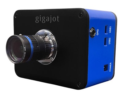
PASADENA, Calif., April 4, 2022 /PRNewswire/ -- Gigajot Technology, inventors and developers of Quanta Image Sensors (QIS), today announced the expansion of its groundbreaking QIS product portfolio with the GJ04122 sensor and associated QIS41 camera. With market leading low read noise, the GJ04122 sensor is capable of photon counting and photon number resolving at room temperature. The QIS41 camera, built around the GJ04122 sensor, pairs well with standard 4/3-inch microscopy optics, bringing unparalleled resolution and low light performance to scientific and industrial imaging applications.
"We are excited about the discoveries that our latest QIS will enable in the life sciences community," said Gigajot's CEO, Dr. Saleh Masoodian, "Additionally, this QIS device further validates that Gigajot has the world's leading small pixel performance which will eventually be deployed to high volume consumer products that value high resolution, low light imaging performance and HDR."
The 41 Megapixel GJ04122 sensor, which was funded in part by the National Science Foundation SBIR Program, utilizes a 2.2-micron pixel and has a read noise of only 0.35 electrons, which is significantly lower than state-of-the-art pixels of similar size. The sensor is capable of photon counting and photon number resolving up to its top speed of 30 frames per second at full resolution. The high resolution and the extremely low read noise provide flexibility for binning and additional post-processing, while maintaining a read noise that is still lower than native lower resolution sensors. While pushing the limits of low light imaging, the GJ04122 sensor also offers an impressive single-exposure dynamic range of 95 dB by utilizing Gigajot's patented high dynamic range pixel.
The QIS41 is a fully featured scientific camera based on the GJ04122 sensor. The QIS41 camera has a SuperSpeed USB 3.0 interface and is capable of true photon counting at room temperature. For more information, or to schedule a virtual demonstration contact Gigajot Sales at www.gigajot.tech/order. The QIS41 camera can be pre-ordered now for Q4 2022 deliveries.
About Gigajot Technology, Inc.: Headquartered in Pasadena, CA, Gigajot is developing the next generation of image sensors. Gigajot's mission is to develop innovative Quanta Image Sensor (QIS) devices and advance this technology for the next generation of image sensors, offering high-speed and high-resolution single-photon detection to realize new, unprecedented image capture capabilities for professionals, and consumers. At Gigajot, every photon counts. For more information, visit www.gigajot.tech.
Press release: https://www.prnewswire.com/news-releases/gigajot-announces-the-worlds-highest-resolution-photon-counting-sensor-301516410.html
Monday, April 11, 2022
MojoVision Announces New Contact Lens Prototype
From TechCrunch News and MojoVision Blog:
The Bay Area-based firm [MojoVision] announced a new prototype of its augmented reality contact lens technology. The system is based around what Mojo calls “Invisible Computing,” its heads up display technology that overlays information onto the lens. Essentially it’s an effort to realize the technology you’ve seen in every science-fiction movie from the past 40+ years. The set-up also features an updated version of the startup’s operating system, all designed to reduce user reliance on screens by — in a sense — moving the screen directly in front of their eyes.
[The] new prototype of Mojo Lens incorporates numerous industry-first features, including the world’s smallest and densest dynamic display, low-latency communication, and an eye-controlled user interface.
The company continues to work with the FDA to help bring the tech to market as part of its Breakthrough Devices Program. The company also announced previous partnerships with fitness brands like Adidas Running to develop workout applications for the tech.
MojoVision Blog: https://www.mojo.vision/news/we-have-reached-a-significant-milestone-blog
TechCrunch Article: https://techcrunch.com/2022/03/30/mojo-vision-takes-another-step-toward-ar-contact-lenses-with-new-prototype/
Friday, April 08, 2022
Yole report on 3D imaging technologies
Full article here: https://www.i-micronews.com/will-3d-depth-cameras-return-to-android-phones/
Some excerpts:
Apple started using structured light for facial recognition technology in the iPhone X in 2017, ushering in an era of 3D depth imaging in the mobile field. Within the next year, in 2018, Android players Oppo, Huawei, and Xiaomi also launched front 3D depth cameras, using very similar structured light technologies to Apple.
The Android camp attempted to use another 3D imaging technology, indirect Time of Flight (iToF). It was used for rear 3D depth cameras, for quick focus and imaging bokeh and some highly anticipated AR games and other applications.
The hardware for this technique is more compact than structured light, requiring only a ToF sensor chip, and a flood illuminator. The distance is computed by the time difference between emission and reception. Compared to structured light, it does not need much computing power, software integration is relatively simple, and overall, it has cost advantages.
LG, Samsung and Huawei used this kind of technology both for front and/or rear implementations.
For a while, no Android player included 3D depth cameras in their flagship phones. However, during Mobile World Congress 2022, Honor unexpectedly released the Magic 4 Pro with a 3D depth camera on the front of the phone. Will 3D depth cameras return to Android phones?
Market report: https://www.i-micronews.com/products/3d-imaging-and-sensing-technology-and-market-trends-2021/
Thursday, April 07, 2022
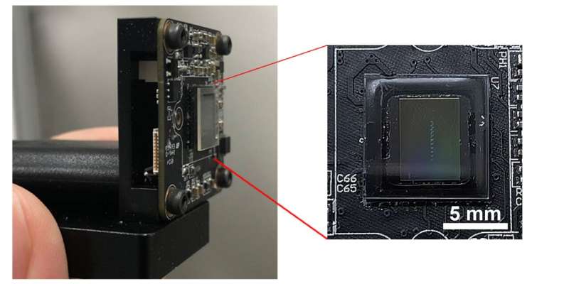
Microsoft Surface Hub 2 Camera

Wednesday, April 06, 2022
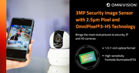
OMNIVISION’s New 3-megapixel Image Sensor
SANTA CLARA, Calif.--(BUSINESS WIRE)--OMNIVISION, a leading global developer of semiconductor solutions, including advanced digital imaging, analog and touch & display technology, today announced the new OS03B10 CMOS image sensor that brings high-quality digital images and high-definition (HD) video to security surveillance, IP and HD analog cameras in a 3-megapixel (MP) 1/2.7-inch optical format.
The OS03B10 image sensor features a 2.5µm pixel that is based on OMNIVISION’s OmniPixel®3-HS technology. This high-performance, cost-effective solution uses high-sensitivity frontside illumination (FSI) for true-to-life color reproduction in both bright and dark conditions.
“Many of our customers already use our OS02G10, an FSI based 2MP 1/2.9-inch image sensor, for security and video applications, such as IP cameras, baby monitors, doorbell cameras, smart TVs, dashcams and more,” said Cheney Zhang, senior marketing manager, OMNIVISION. “The OS03B10 is pin-to-pin compatible with OS02G10, enabling our customers to seamlessly upgrade their security products to a 3MP image sensor, greatly improving image capture and HD video without any redesigns.”
By leveraging an advanced 2.5µm pixel architecture, the OS03B10 achieves excellent low-light sensitivity, signal-to-noise ratio, full-well capacity, quantum efficiency and low-power consumption. It can capture videos in a 16:9 format at 30 frames per second. Default and programmable modes allow for a more convenient way of controlling the parameters of frame size, exposure time, gain value, etc. It also offers image control functions such as mirror and flip, windowing, auto black level calibration, defective pixel correction, black sun cancellation and more. The OS03B10 supports DVP and MIPI interfaces.
Samples of the OS03B10 are available now and will be in mass production in Q2 2022. For more information, contact your OMNIVISION sales representative: www.ovt.com/contact-sales.
Link: https://www.businesswire.com/news/home/20220330005300/en/OMNIVISION%E2%80%99s-New-3-megapixel-Image-Sensor-with-OmniPixel%C2%AE3-HS-Brings-the-Most-Vivid-Pictures-to-Security-IP-and-HD-Cameras
Monday, April 04, 2022
Hamamatsu videos
Hamamatsu has published new videos on their latest products and technologies.
Mini Spectrometers: What are mini-spectrometers and how can they be used in the medical industry?
Sunday, April 03, 2022
Better Piezoelectric Light Modulators for AMCW Time-of-Flight Cameras
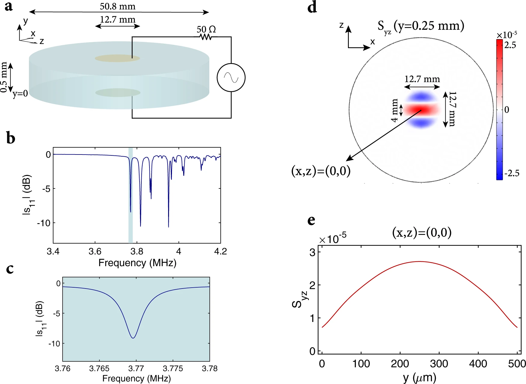
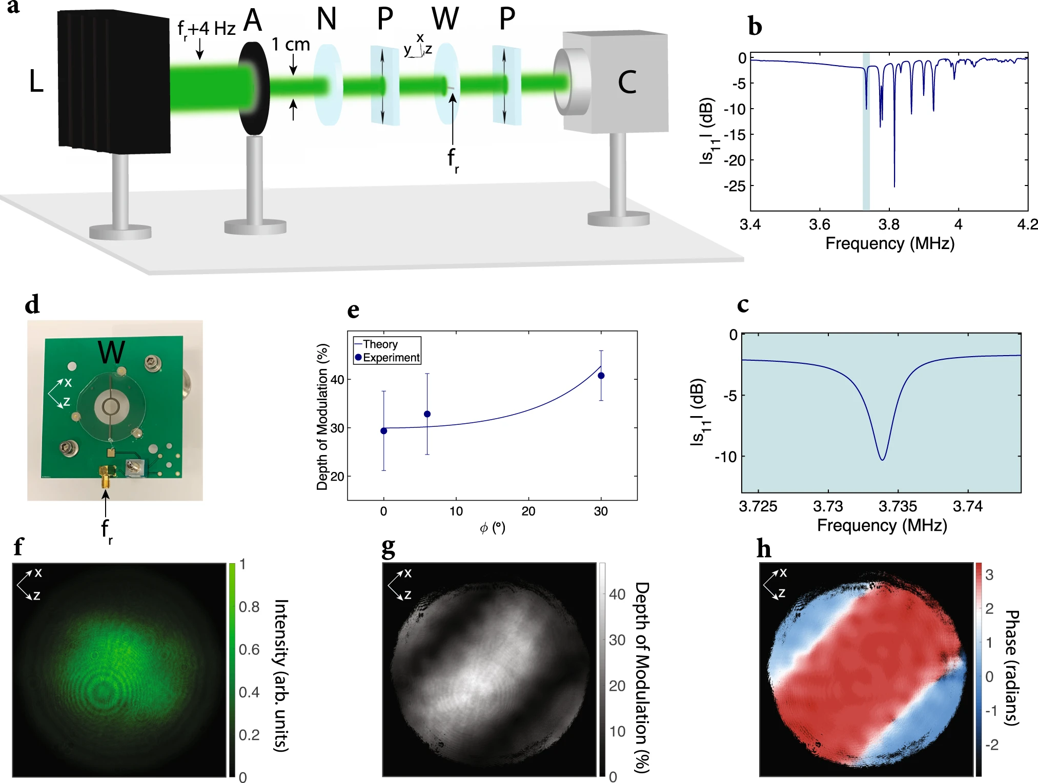
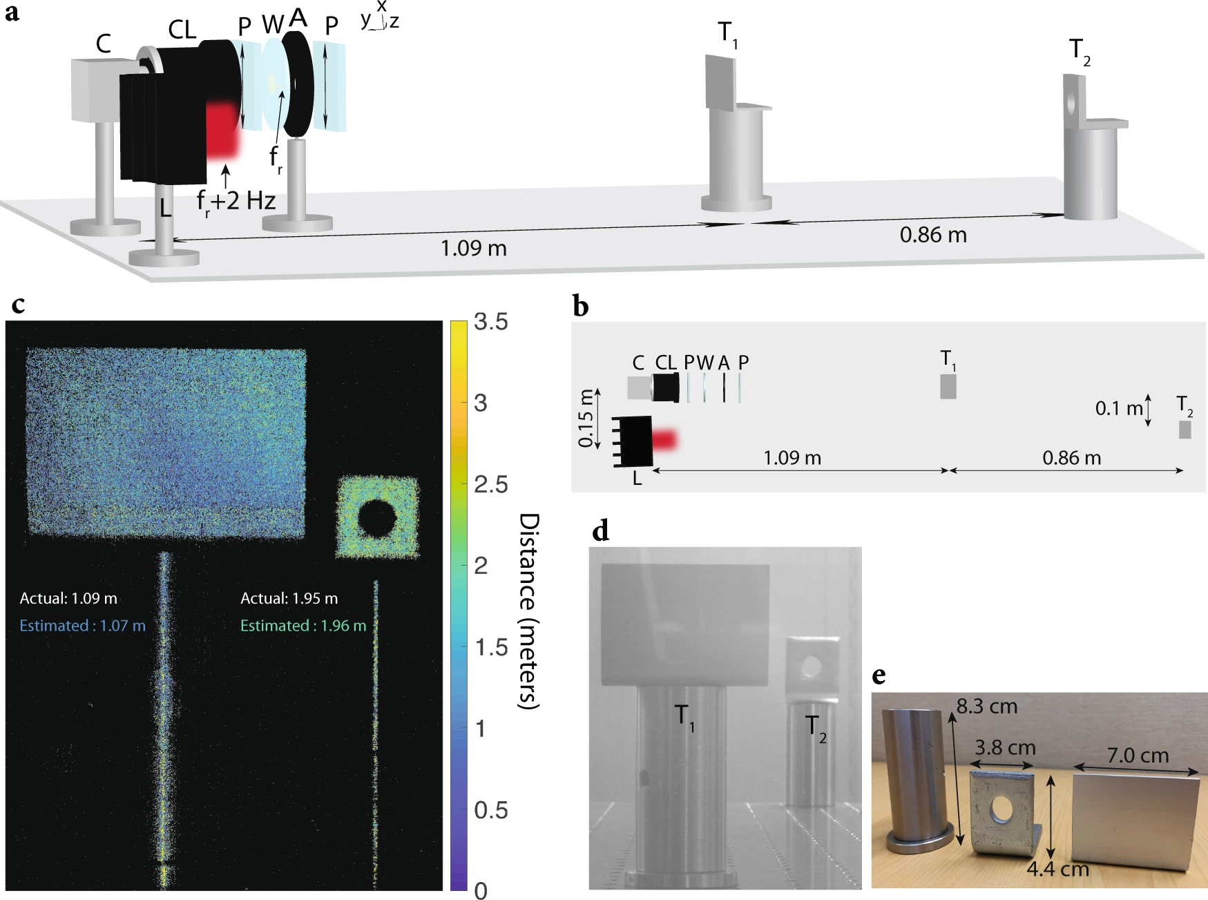
A team from Stanford University's Laboratory for Integrated Nano-Quantum Systems (LINQS) and ArbabianLab present a new method that can potentially convert any conventional CMOS image sensor into an amplitude-modulated continuous-wave time-of-flight camera. The paper titled "Longitudinal piezoelectric resonant photoelastic modulator for efficient intensity modulation at megahertz frequencies" appeared in Nature Communications.
Intensity modulators are an essential component in optics for controlling free-space beams. Many applications require the intensity of a free-space beam to be modulated at a single frequency, including wide-field lock-in detection for sensitive measurements, mode-locking in lasers, and phase-shift time-of-flight imaging (LiDAR). Here, we report a new type of single frequency intensity modulator that we refer to as a longitudinal piezoelectric resonant photoelastic modulator. The modulator consists of a thin lithium niobate wafer coated with transparent surface electrodes. One of the fundamental acoustic modes of the modulator is excited through the surface electrodes, confining an acoustic standing wave to the electrode region. The modulator is placed between optical polarizers; light propagating through the modulator and polarizers is intensity modulated with a wide acceptance angle and record breaking modulation efficiency in the megahertz frequency regime. As an illustration of the potential of our approach, we show that the proposed modulator can be integrated with a standard image sensor to effectively convert it into a time-of-flight imaging system.
Friday, April 01, 2022
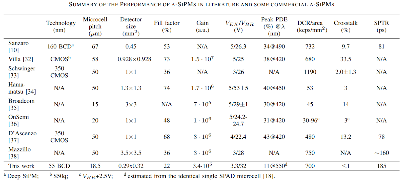
Two new papers on 55 nm Bipolar-CMOS-DMOS SPADs
The AQUA research group at EPFL together with Global Foundries have published two new articles on 55 nm Bipolar-CMOS-DMOS (BCD) SPAD technology in the upcoming issues of IEEE Journal of Selected Topics in Quantum Electronics.







:format(webp):no_upscale()/cdn.vox-cdn.com/uploads/chorus_asset/file/23336437/SH_Smart_Camera___Live_3.jpg)
