Monday, May 31, 2021

Sony about Polarization Sensor Design Challenges

Sony publishes an interview with its polarization-sensitive image sensor designers. Few quotes:

How did you overcome the problem of the incompatibility between the extinction ratio and transmittance?
Yamazaki: Initially, the gaps between the fine strips of polarizer were filled in with oxidation film from the viewpoint of the stability and reliability of the processes, but it turned out that this method was an obstacle for solving the incompatibility problem. Theoretically, both the extinction ratio and transmittance can be improved by making the polarizer sufficiently finer than the light wavelength (i.e., thinner wire grid and narrower gaps), but there is a technical limitation in metal processing. Moreover, the wavelength becomes shorter as the light passes through the oxidation film. We realized that this structural configuration demanded even finer polarizer.
We then came up with the idea to empty the gaps in a polarizer, what we called the air-gap structure. This innovative structure made it possible to solve the problem of incompatibility between extinction ratio and transmittance.
One problem was solved, but an array of other challenges awaited. For example, establishing the stability and reliability of the air-gap structure, nano-order processing to realize a multi-layered structure of polarizer, and mounting this infinitesimal structure on an uneven surface of the image sensor.

What are the future possibilities for polarization image sensors?
Kato: Controlling light is an important factor in obtaining polarization information. We expect that the sensor will be introduced initially in factories, where they are able to control light sources.
For the manufacturing industry, the sensor should hopefully be leveraged more in inspections. Potentially, the polarization image sensor can make significant contributions to such inspections that previously could not be automated or were impractical with ordinary image sensors.
Another promising solution it can offer is the reflection removal on vehicle windows for ITS. Conventional polarizing filters are ineffective for removing reflection on certain vehicle models. I hear that there were some ITS projects that were not realized due to this problem. I hope that our polarization image sensor will make a breakthrough for such cases.

What would you like to try in the future?
Yamazaki: There are the advantages unique to polarization image sensors, but there is a disadvantage in the current state of the device as well, which is that mounting a polarizer compromises the sensor’s sensitivity and image resolution. I would like to pursue the development of a polarization image sensor that overcomes this issue of compromised sensitivity and resolution, broadening the application of this sensor.

Sony Presents ToF Sensor Use Cases

Sony publishes "Life with DepthSense" video:

Hynix "Black Pearl" and "Black Pearl Red" Sensors

SK Hynix has updated its CIS web page with emphasis on "Black Pearl" brand:

Ho-young Cho, Technical Leader (TL) at CIS Marketing Strategy of SK hynix said, “SK hynix officially names all of its CIS products as “Black Pearl” starting from this [2020] year, and plans to continuously introduce products that can deliver the best value to customers in not only the memory semiconductor market, but also the CIS market. We will do our best to establish a position in the CIS market that matches the brand’s meaning, like a black pearl considered as the rarest and the most beautiful pearl among all.

The company's lineup consists of 0.8um, 1.0um, and 1.12um pixel products and only one 2um sensor for security cameras under "Black Pearl Red" brand. Apparently, all other pixel sizes have been discontinued:


Sunday, May 30, 2021

Mid-IR Imaging Use Cases

The newly formed Mid IR Alliance publishes a video on MidIR imaging use cases:
  • An in-car camera could see an alcohol in the driver's breath and block the ignition
  • Adjusting a car fan speed based on CO2 level inside the car
  • Monitor car exhaust emission level
  • Detect explosives from a long distance
  • Greenhouse gases are visible in mid-IR, detection and analysis are possible


Saturday, May 29, 2021

Fight between Velodyne and its Founders Continues

BusinessWire: David Hall, the beneficial owner of approximately 98,951,541 shares or 52.2% of the outstanding common stock of Velodyne Lidar, Inc. issues a statement:

"As the founder of Velodyne Lidar, I have always put the Company’s best interests first. This operating philosophy helped guide my actions and decisions as I led Velodyne Lidar to many years of high growth and success, cementing the Company’s position at the forefront of lidar technology invention and innovation. It gives me great concern to see this commitment now fade in the boardroom and c-suite of the Company I built. I will not stand idly by and watch the Board squander Velodyne Lidar’s bright future with what I believe is a lack of strategic focus and poor corporate governance. That is why Marta and I have nominated Eric Singer – a highly-qualified and independent individual – for election to Velodyne Lidar’s Board.

Marta and I have repeatedly expressed our belief that Velodyne Lidar is at a critical juncture at this point in time. We voiced our grave concerns regarding the Company’s plunging product sales, departure of key R&D personnel, significant loss of market share to competitors, the serious risk of theft of IP in China and the Company’s overall poor financial performance. We believe that the Board has allowed stagnation in innovation to persist, resulting in a lack of new product offerings to meet evolving market demand. Additionally, we believe the Board has overconcentrated limited company resources on executive compensation when capital should instead be invested in research and development.

As disclosed by Velodyne Lidar, the average selling price of existing lidar sensors will continue to decline by as much as 20% in 2021, so the Company’s ability to introduce new products that adapt to changing technology and anticipate future standards is critical to improve its prospects for growth.

In order to maintain its competitive position and take advantage of consolidation opportunities, the Board should have a singular strategic focus. But rather than increasing focus on the addition of new research and development personnel to keep pace with innovation, the current Board instead opted to increase G&A expenses significantly. G&A expenses increased by 59% for the three months ended March 31, 2021 from the comparable period of 2020. This is in the face of Velodyne Lidar’s 35% decline in product revenues for the comparable periods of March 31, 2020 to March 31, 2021.

In our view, the status quo at Velodyne Lidar is unacceptable. Poor leadership and weak financial performance are not a recipe for success in the public markets."

BusinessWire: Velodyne responds: "The Company believes its pipeline is the most robust in the industry, as demonstrated by a 51% increase in projects – growing from 131 projects in January 2020 to 198 as of May 2021. Velodyne Lidar shipped over 2,600 sensors in the first quarter of 2021 alone, including 600 solid state sensors. Based on available public information, this far exceeded shipments of all of the Company’s public competitors combined.

In recent months, Velodyne’s Chief Executive Officer, Dr. Anand Gopalan, PhD, and Board have continued to bolster the Company’s leading executive team with a focus on maintaining its position as the most innovative lidar company in the industry. Supporting Velodyne Lidar’s executives is a world-class engineering team with more than 120 engineers on staff.

The Velodyne Lidar Board prides itself on its commitment and adherence to sound corporate governance, seeking highly qualified, independent and diverse directors. The Halls have put forward a candidate in Eric Singer who the Board believes exemplifies none of those characteristics. The Board determined not to recommend Mr. Singer for election at the upcoming Annual Meeting of Stockholders following a comprehensive process to evaluate Mr. Singer, including reviewing his qualifications and prior experience.

The Board is committed to upholding the highest standards of corporate governance. That commitment is evidenced by the Board’s responses to various proposals made by the Halls in December 2020 that would have had the effect of enhancing the Halls’ control over the Company."

Few slides from the company's recent Q4 2020 investor presentation:

Friday, May 28, 2021

Canon Article about its 1MP SPAD Sensor

Canon publishes Featured Technology article about its 1MP SPAD sensor:

"Until recently, it was considered difficult to create a high-pixel-count SPAD sensor. On each pixel, the sensing site (surface area available for detecting incoming light as signals) was already small. Making the pixels smaller so that more pixels could be incorporated in the image sensor would cause the sensing sites to become even smaller, in turn resulting in very little light entering the sensor, which would also be a big problem.

Specifically, on conventional SPAD sensors, structural demands made it necessary to leave some space in between the different sensing sites on neighboring pixels. The aperture ratio, which indicates the proportion of light that enters each pixel, would therefore shrink along with the pixel size, making it difficult to detect the signal charge.

However, Canon incorporated a proprietary structural design that used technologies cultivated through production of commercial-use CMOS sensors. This design successfully kept the aperture rate at 100% regardless of the pixel size, making it possible to capture all light that entered without any leakage, even if the number of pixels was increased. The result was the achievement of an unprecedented 1,000,000-pixel SPAD sensor."


"The SPAD sensor that Canon has developed is also equipped with a global shutter that can capture videos of fast-moving subjects while keeping their shapes accurate and distortion-free. Unlike the rolling shutter method that exposes by activating a sensor’s consecutive rows of pixels one after another, the SPAD sensor controls exposure on all the pixels at the same time, reducing exposure time to as short as 3.8 nanoseconds3 and achieving an ultra-high frame rate of up to 24,000 frames-per-second (FPS) in 1-bit output. This enables the sensor to capture slow motion videos of phenomena that occur in extremely short time frames and were previously impossible to capture."

Pixart Unveils Gesture Recognition Solution

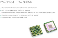
EETimes: PixArt’s offers Multi-Object Gesture Recognition set consisting of a Global Shutter 400x400 pixel sensor (PAC7640LT) with a 120fps frame rate, and a standalone ISP SoC (PAG7661QN) with full algorithmic support to offer our customers a painless journey in end-product development.

Microsoft about iToF System Design

Microsoft continues a servies of posts about its iToF Azure platform. The latest post "Time of Flight Camera – System Overview" is co-authored with Analog Devices team:

"Analog Devices (ADI) is building on the core Microsoft ToF pixel technology to deliver complete ToF solutions to a broad customer base in areas such as industrial factory automation, inventory management, automotive infotainment, augmented reality, computational photography and videography."

Thursday, May 27, 2021

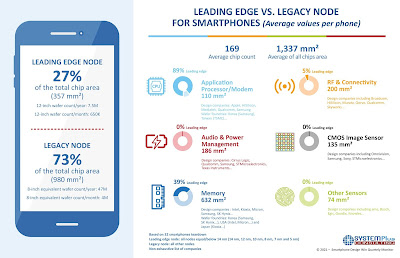
Image Sensors Occupy 10% of Smartphone Silicon Area

EETimes: According to SystemPlus statistics, 10% of average smartphone silicon area are image sensors (not including optical fingerprint sensors.)

Wednesday, May 26, 2021

Now it's Official in English: Omnivision Launches First 0.61um Pixel Product

BusinessWire: Reported in China more than 2 weeks ago, Omnivision's 60MP OV60A with the world’s smallest 0.61µm pixel is now announced in English.

The OV60A can fit into a 1/2.8 inch optical format in either 3:4 or 16:9 aspect ratio configurations. The 4-cell color filter array on the OV60A uses near pixel binning to output up to 15MP images with 4X the sensitivity offering 1.22µm equivalent performance for preview and native 4K video with extra pixels for EIS. The sensor also supports low power mode for “always on” sensing that can save precious battery life when paired with the phone’s artificial intelligence functions.

In 2022, TSR estimates there will be 43 million image sensors with 40MP+ resolution for front facing cameras and over 350 million image sensors with 50MP+ resolution for rear facing cameras shipped to smartphone manufacturers,” said Arun Jayaseelan, staff marketing manager at OmniVision. “The OV60A with 60MP resolution packed into a small form factor is an attractive option for high resolution front facing cameras as well as for ultra-wide rear facing cameras on mobile phones.

The new 0.61µm pixel is 24 percent smaller in area than the previous generation 0.7µm pixel solution, yet it can achieve higher QE with better crosstalk and angular response than the 0.7µm generation. The OV60A can output 15MP or 4K2K with EIS resolutions at 60 fps and supports staggered HDR timing for high dynamic range video enablement. The “always on” low power modes include an ambient light sensing mode for wake up as well as a low power streaming mode. This sensor also can support dual I/O voltage rails (1.8V and 1.2V) as well as CPHY interface.

Samples of the OV60A are now available.

Technavio Forecasts Automotive CIS Market Growth

PRNewswire: Technavio forecasts automotive image sensors market to grow by $4.91B, registering a CAGR of almost 29% during 2021-2025.

Sony and TSMC to Build 20nm Joint Fab in Japan

Reuters reports that Japan's government is in talks with TSMC and Sony to build the country's first 20nm fab in Japan. The two companies are expected to invest 1 trillion yen ($9.2 billion) into this project. The potential factory would be built close to Sony's image sensor fab in southwest Japan, according to a proposal floated by Japan's trade and industry ministry.

Sony has held a Corporate Strategy Meeting today. The company presents its ambitious investment plans, albeit in a general form without explicitly mentioning TSMC and 20nm:

Tuesday, May 25, 2021

CEA-Leti Unveils "Always-On" Image Sensor with Face Recognition

CEA-Leti announces what it calls the world's first autonomous imager technology that activates smartphones and small appliances through face recognition or other specific patterns.

Called µWAI (micro-WAY) and sized as small as a 1€ coin, the autonomous imager features a novel readout and processing architecture co-designed with an optimized algorithmic pipeline, in which the recognition results from a sequence of elementary algorithms, to provide ultralow-power wake-up modes and compact silicon implementation to keep costs down. 

It is the first smart image sensor jointly featuring auto-exposure for all lighting conditions and 88dB dynamic range, as well as motion detection and feature extraction for event-based functioning, and AI-based object recognition that triggers highly reliable identification. These key features also enable highly reliable decision taking for a few tens of pJ/pixel/frame, which outperforms existing off-the-shelf systems. The pJ/pixel/frame measures the energy spent by each pixel for each single image within a frame of images. A typical implementation requires about 10,000 times more energy than µWAI.

The autonomous imager is the world's first highly efficient, compact and ultralow-power, smart-awaken system designed for everyday small appliances. It also includes:
  • Energy efficiency: consuming 10k less than low-power camera plus processor set,
  • Privacy-compliant, AI-based recognition: nearly human-detection performance (95 percent),
  • Wide operating lighting sensitivity to ensure accurate recognition in extremely variable conditions,
  • Five-year, always-on CR1025 battery lifetime, and
  • 3-6µW operation, which is required for the Internet of Things and can work with a button cell that lasts five years.
Applications and functions include automatic switching and face identification in mobile devices, contact-less smart switching of household appliances and sport-and-entertainment devices in smart homes. µWAI also provides face recognition, people counting, alarm triggering in smart buildings, vehicle-interior situation awareness, driver identification, parking-situation awareness and a smart-unlocking system in automobiles.

"The recognition engine is optimized to recognize faces when movement is detected. CEA-Leti's team is working hand-in-hand with STMicroelectronics to develop specific smart-imager products as we consider extending the technology to other use cases," said Antoine Dupret, CEA-Leti's industrial partnership manager. "We target adapting the recognition engine as IP embedded in various cameras and optimizing the performance of the imager to the requirements of our partner's customers."

Omnivision Unveils 2MP "Always-On" Sensor

BusinessWire: OmniVision announces the industry’s first 1/7-inch stacked 2MP sensor, the OV02C, for video conferencing in thin bezel premium notebooks, tablets and IoT devices. The sensor offers 60 fps in the thinnest 3mm module Y size for high screen-to-body ratio designs.

The OV02C’s “Always On” feature senses user presence in ultra-low-power mode and the system can be locked and woken up touchlessly, extending the lifetime of the battery.

Opnous Raises $15M Investment

EETimes-China: iToF sensor maker Opnous (Shanghai Juyou Intelligent Technology Co., Ltd.) announces the completion of a B round of equity financing of over 100M yuan (about $15.6M)

Monday, May 24, 2021

Yet Another Samsung 108MP Promotional Video

Samsung publishes yet another promotional video of its 108MP HM3 sensor that was first announced in January 2021:

dToF Rx Model


"A histogram of photon return times is measured and then processed to estimate object depth. By collecting many photons that span multiple bins of the histogram the final depth estimate interpolates between time-to-digital converter (TDC) bins to produce a result that is more precise than the converter resolution. The precision of this interpolation depends on the temporal spread of the measurement, the resolution of the TDC, and the number of signal and background photons measured. There is a need for dToF depth precision models to guide design and predict and tune performance during use. In this article, we present models that estimate sensor depth precision versus dToF design parameters and photons measured. We use Monte Carlo simulations and experimental measurements to prove the accuracy of the models. With proven models in hand, we investigate a dToF sensor design by first presenting the dependence of precision upon the TDC resolution and the signal-to-noise ratio. Second, we experimentally measure the depth precision versus the intensity of background illumination. The models closely match the measurements of background susceptibility and locate a transition point of background intensity below which precision is constant and above which the precision continuously degrades. Finally, experimental measurements demonstrate how the modeling enables dynamic tuning: from a single histogram we estimate precision, thus enabling sensor exposure time tuning for a target precision or prediction of the precision given a change in object distance or background illumination."

dpiX Develops Flexible X-Ray Sensors

dpiX announces its continued cooperation with the U.S.DoD in the next-stage development and production of polyimide-based, flexible optical sensor technologies that will support DoD explosive ordnance disposal applications. This milestone marks the final steps of this flexible X-ray project buy-plan that was competitively awarded to dpiX in 2017.

dpiX operates the largest and most sophisticated flat panel semiconductor plant outside of Asia, and is said to be the worldwide market leader in optical sensors for radiography (a-Si/IGZO). dpiX strives to be the number one partner for U.S. technology companies to design, prototype and manufacture all kinds of flat panel semiconductors in its trusted U.S. semiconductor facility in Colorado Springs, Colo. dpiX and its strategic partners are currently pursuing support under the Creating Helpful Incentives to Produce Semiconductors for America (CHIPS) Act (as incorporated under the Biden administration’s infrastructure plan) to strengthen the U.S. flat panel foundry business.

We are working in close technology cooperation with dpiX that will bring their new state-of-the-art flexible optical sensor technology within reach of our U.S. Armed Forces. Having an established and trusted manufacturing partner for this in the U.S. is of utmost importance in becoming less dependent on foreign value-chains,” said Keith DeVries, Program Manager, Manufacturing Science and Technology.

Sunday, May 23, 2021

Sony SenSWIR Reverse Engineered

TechInsights publishes a nice analysis "Groundbreaking SenSWIR Sensor by Sony - IMX990/IMX991."

"By moving away from pixel-level bump bonds and taking advantage of greater miniaturization in Cu-Cu Direct Bond Interconnect (DBI), Sony was able to reduce the pixel size of the InGaAs/ROIC SWIR imagers down to 5.0 µm. This makes the IMX990/IMX991 the smallest pixel-pitch InGaAs-based SWIR image sensors commercially available on the market.

Sony Semiconductor Solutions Die-to-Wafer Hybridization Advanced Packaging Process
Additionally, Sony has developed a highly scalable Die-to-Wafer Hybridization process, with wafer-level hybrid bonding to help manufacture its new SWIR imagers. In Die-to-Wafer Hybridization, a handle wafer supports an array of pre-manufactured SWIR InGaAs Die so that hybrid bonding can take place much like conventional CMOS Image Sensors CIS-to-ISP wafer-level bonding.

This approach presents two advantages, the Cu-Cu DBI can help reduce the overall height of the Die while Die-to-Wafer hybridization can help reduce the per-Die cost, thereby facilitating greater utilization of Sony’s SWIR technology for a wide range of applications."