Full blog article here: https://www.techinsights.com/blog/apple-iphone-14-image-sensor-preliminary-analysis
- Real-time point cloud and depth map.
- Resolution: 240x180@30fps on RPI4/CM4
- Up to 4M measuring distance
- Onboard 940nm laser for both indoor & outdoor uses, no external light source needed.
- V4L2-based video kernel device
- C/C++/Python SDK for userland depth map output and example source code
- ROS ready
- 38 x 38mm board size


Kickstarter link: https://www.kickstarter.com/projects/arducam/time-of-flight-tof-camera-for-raspberry-pi
From the VISION 2022 exhibition in Stuttgart:
AlpsenTek® launches the ALPIX-Eiger™, a fusion vision sensor for high-end imaging
AlpsenTek®, a leading developer of fusion vision sensors, announced the launch of the ALPIX-Eiger™ fusion vision sensor chip, specifically designed for high-end imaging applications. Using the original patented Hybrid Vision™ fusion vision technology, ALPIX-Eiger™ enables the fusion of image sensing and event sensing at the pixel level, making the simultaneous output of both image and event streams possible.
ALPIX-Eiger ™ is a patented chip architecture and pixel design with advanced 3D stacking and BSI back-illuminated/backlight technology. With a pixel size of just 1.89µm×1.89µm and a resolution of 8.0 megapixels, it is the smallest pixel size and highest resolution image sensor with event-aware capabilities in the industry. It offers broad application capabilities to small-sized smart devices, such as mobile phones and motion cameras.
High performance
The ALPIX-Eiger™ not only maintains the advantages of image sensors, ensuring full image quality and rich image details but also facilitates event sensing through the patented design of digital-analog mixed signal processing in pixels. This technology allows single pixel to work independently to detect light changes. Having a response speed of microseconds, high frame rate (equivalent to 5000fps), high dynamic range (110dB), low data redundancy and other characteristics helps the image sensor obtain more information and enhances image quality. Compared with previous event camera solutions, the event stream output by ALPIX-Eiger™ carries color information, which aids color reconstruction of the image and achieves better quality photo and video capabilities.
Wide Applications
In practical applications, intelligent imaging devices equipped with ALPIX-Eiger™ chips can achieve high-end functions such as de-blurring, high frame rate, and super-resolution to facilitate the development of more visual applications. The HDR performance and instantaneous response of the ALPIX-Eiger™ also allow the device to obtain better imaging results at night in scenarios with extreme light and dark contrasts.

Other recent posts about Alpsentek:
https://image-sensors-world.blogspot.com/2022/06/alpsentek-vision-sensor-startup-raises.html
https://image-sensors-world.blogspot.com/2021/11/interview-with-ceo-of-ruisi-zhixin.html
http://image-sensors-world.blogspot.com/2021/10/chinese-startup-ruisizhixin-develops.html
Recent EE Journal article suggests that the 2nd generation time-of-flight proximity sensor from STMicro uses metalenses designed by Metalenz, a Harvard spinoff.
Original article here: https://www.eejournal.com/article/time-of-flight-sensors-trilobites-and-tunable-optics-what-an-unlikely-combo/
Some excerpts below:
Time of Flight Sensors, Trilobites, and Tunable Optics – What an Unlikely Combo!
STMicroelectronics has added a new member to its line of VL53 FlightSense TOF (time of flight) distance/ranging sensors, but this new sensor takes a radical departure from the previous generation by replacing a conventional lensing system with metalenses, developed in conjunction with a startup company called Metalenz and based on technology originally developed in a Harvard University metamaterial lab. According to Metalenz, this is the first commercial product to incorporate its metalens technology.
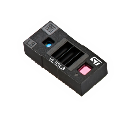
The resulting TOF sensor can achieve more than double the range – as much as 4m in indoor settings – or it can operate at half the power consumption relative to ST’s previous generation of VL53 TOF sensors. The expanded range and reduced power consumption arise from a combination of a more efficient VCSEL driver circuit and the improved light-gathering ability of the metalens covering the SPAD array. ST’s announcement did not specify a minimum target distance for the VL53L8 sensor, but its predecessor, the VL53L5CX sensor, has a minimum ranging distance of 2cm and an apparent resolution of 1mm, with ±15mm accuracy in the 20-200mm range and 4-11% in the 201-4000mm range, depending on ambient lighting.
Like the earlier VL53L5CX sensor, the new VL53L8 sensor can determine distance to a target or multiple targets simultaneously using either 16 zones at 60Hz or 64 zones at 15Hz, as observed through a 43.5° x 43.5° square field of view. An integrated microcontroller in the TOF sensor delivers range-to-target information directly over an I2C or SPI serial interface and can generate interrupts to wake a host processor when each distance reading is made. Even with all it packs inside, this is a physically tiny sensor, measuring 6.4 x 3.0 x 1.75 mm. It’s supplied as a single, factory-aligned, reflowable component so you can drop it into a variety of products, even small portable ones.
A recent press-release from Metalenz confirms that they have indeed partnered with ST on the new VL53L8 proximity sensor.
Press release: https://www.metalenz.com/the-worlds-first-metasurfaces-have-arrived-on-the-market/
Boston, MA and Geneva, Switzerland – June 9, 2022 – Metalenz, the first company to commercialize meta-optics, and STMicroelectronics (NYSE: STM), a global semiconductor leader serving customers across the spectrum of electronics applications, today announce that ST’s currently released VL53L8 direct Time-of-Flight (dToF) sensor is the highly anticipated market debut of the meta-optics devices developed through their partnership, which was disclosed in June 2021.
Metalenz’s Harvard-born, meta-optics technology can replace existing complex and multi-element lenses and provide additional functionality with a single meta-optic embedded in time-of-flight (ToF) modules from ST, the leading company in supplying 3D sensing modules. The introduction of Metalenz technology in these modules brings performance, power, size, and cost advantages to a multitude of consumer, automotive, and industrial applications. This marks the first time metasurface technology is commercially available and being used in consumer devices.
Unlike traditional molded and curved lenses, Metalenz’s novel optics are completely planar. Planar metasurface optics are now being manufactured on silicon wafers alongside electronics in ST’s semiconductor front-end fabs for the first time. The meta-optics collect more light, provide multiple functions in a single layer, and enable new forms of sensing in smartphones and other devices, while taking up less space. Metalenz’s flat-lens technology replaces certain existing optics in ST’s FlightSense™ ToF modules, which serve applications such as smartphones, drones, robots, and vehicles. In these, ST has sold more than 1.7 billion units to date.
“More than a decade of foundational research has brought us to this point. Market deployment of our meta-optics makes this the first metasurface technology to become commercially available,” said Rob Devlin, co-founder and CEO of Metalenz. “ST’s technology, manufacturing expertise, and global reach allow us to impact millions of consumers. We have multiple wins that mark the first application of our platform technology and we are now designing entire systems around its unique functionality. Our meta-optics enable exciting new markets and new sensing capabilities in mobile form factors and at a competitive price.”
Optics.org news: https://optics.org/news/13/9/18
13 Sep 2022
Yole Intelligence says that Sony is looking to consolidate its leading position as the market begins a new growth cycle.
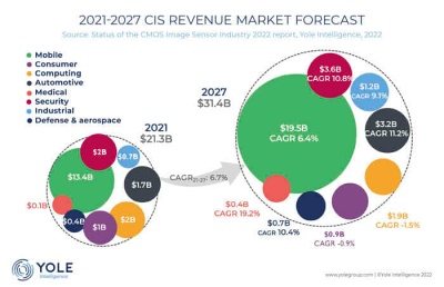
Analysts at Yole Intelligence, the France-based research market company, are predicting that the market for CMOS image sensors is about to begin a new phase of growth - and will be worth more than $31 billion by 2027.
If correct, it would represent a compound annual growth rate (CAGR) of nearly 7 per cent, with the sector recovering from a slump caused by US sanctions on Chinese vendors.
That rate of growth is expected to be propelled primarily by applications in smart phones - the largest single end market for the devices - as well as emerging use cases in the automotive sector and security imaging.
Solid growth
Yole says that the market for CMOS image sensors grew nearly 25 per cent in 2019 - with buyers partly responsible for creating a bubble as they stockpiled devices in advance of those sanctions taking effect.
In 2020 the rate of growth slowed to just over 7 per cent, before the combination of sanctions and supply-chain effects resulting from the Covid-19 pandemic saw growth drop to just 2.8 per cent in 2021.
However, a recovery appears to have begun in the closing quarter of 2021, which is said to have been the best ever in terms of CMOS image sensor production. The market ended up being worth $21.3 billion that year, thinks Yole.
“A new growth cycle is now expected, supported by opportunities in mobile and other markets such as automotive and security imaging,” stated the firm. “In the coming years the [CMOS image sensor] industry growth will at least match the general semiconductor [industry] growth rate, reaching $31.4 billion by 2027 with a 6.7 per cent CAGR.”
According to the analyst team’s figures, mobile phone applications accounted for $13.4 billion in sales in 2021, almost two-thirds of the total market for CMOS image sensors. That sub-sector is expected to grow at a CAGR of more than 6 per cent through 2027, reaching close to $20 billion.
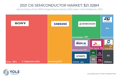
Yole analyst Florian Domengie observed: “The [CMOS image sensor] ecosystem is still dominated by historical leaders. Sony, Samsung, OmniVision, and STMicroelectronics are all strong players in mobile and consumer markets.”
Market shares
The analyst firm’s figures indicate that Sony claimed the leading market share of 39 per cent in 2021, putting it ahead of Samsung (22 per cent), OmniVision (13 per cent), and STMicroelectronics (6 per cent).
However, that Sony figure is historically low, and the Japanese technology giant is now making efforts to increase it significantly.
“As a consequence of Covid-19 and the US Huawei ban, Sony’s market share faltered in 2021,” Yole explains. “That allowed its competitors to raise their game and play technology catch up.
“However, in June 2022, Sony confirmed its ambition to reclaim its market share, aiming at 60 per cent by 2025. This announcement should reinforce production capacity and research and development [spending] in the coming years.”
In its latest quarterly results announcement, Sony said that its sales of image sensors had been impacted by a slump in the Chinese smart phone sector, but added that it was expecting growing adoption of CMOS sensors with larger die sizes and higher resolution.
"In addition, due to an easing supply and demand equilibrium for logic semiconductors, it has become possible to gradually increase the production of high-value-added image sensors, the production of which was previously restricted due to supply constraints," Sony also pointed out.
The Yole report suggests that the leading Chinese manufacturers - OmniVision, GalaxyCore, and SmartSens - have responded well to the Huawei sanctions, and are now outperforming the competition.
Although its corporate headquarters is in Silicon Valley, and it used to be listed on the Nasdaq, OmniVision was acquired by a consortium of Chinese private equity investors in 2016 - and has since been sold to Shanghai-based Will Semiconductor.
Yole says that of the other Chinese players GalaxyCore is strengthening its position, approaching $1 billion in annual revenues and ranking fifth in the market, just ahead of US-based Onsemi.
Next comes Korea’s SK Hynix with a 3 per cent market share, and SmartSens with 2 per cent. Japan’s Canon and US defense group Teledyne round out the top ten suppliers, with Hamamatsu and Panasonic earning similar shares in 2021.
FLIR has published an updated version of their "periodic table" of machine vision sensors: https://www.flir.com/discover/iis/machine-vision/sensor-periodic-table/
The full table features CCD and CMOS image sensors across various manufacturers including Sony, e2v, Onsemi, SHARP, Canon, CMOSIS, OmniVision, Gpixel and Aptina.
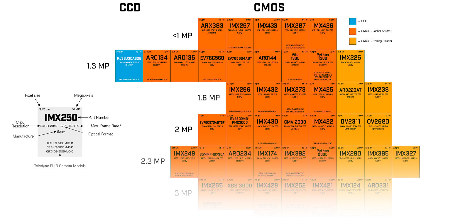
Updated for 2022 - The Teledyne machine vision sensor periodic table is a useful resource for system designers looking to quickly compare sensor specifications including resolution, pixel size, frame rates and optical formats. Now with more than 100 widely used machine vision sensors including third generation Sony Pregius, fourth generation Sony Pregius S, e2v, onsemi, OmniVision, CMOSIS, and GPixel, this periodic table also visually differentiates CCD, CMOS rolling and CMOS global shutter sensors.
With so many sensors to choose from, we understand that it could be tricky to keep track of them. This handy resource organizes currently available machine vision sensors in an easy-to-understand colour coded periodic table with an overview of important specifications. We suggest printing this free poster and pinning it up on your wall for easy reference.
From Businesswire --- "OMNIVISION Announces World’s Smallest Global Shutter Image Sensor for AR/VR/MR and Metaverse".
OmniVision has announced the industry’s first and only three-layer stacked BSI global shutter (GS) image sensor. The OG0TB is the world’s smallest image sensor for eye and face tracking in AR/VR/MR and Metaverse consumer devices, with a package size of just 1.64mm x 1.64mm, it has a 2.2µm pixel in a 1/14.46-inch optical format (OF). The CMOS image sensor features 400×400 resolution and ultra-low power consumption, ideal for some of the smallest and lightest battery-powered wearables, such as eye goggles and glasses. Ultra-low power consumption is critical for these battery-powered devices, which can have 10 or more cameras per system. Their OG0TB BSI GS image sensor consumes less than 7.2mW at 30 frames per second (fps).
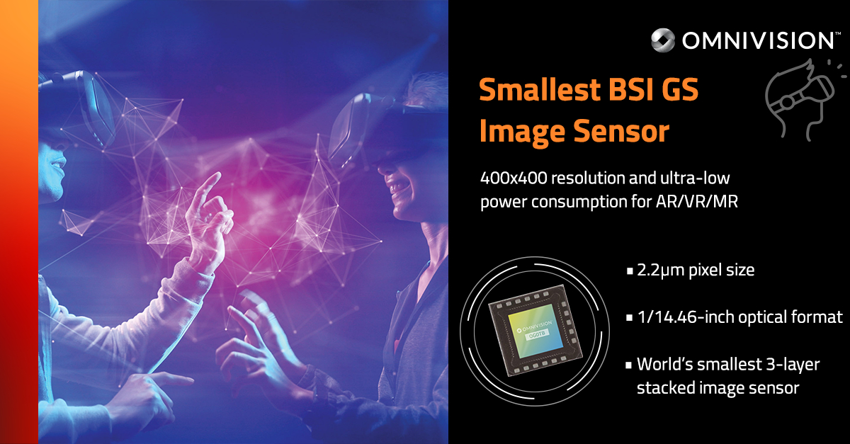
SANTA CLARA, Calif.--(BUSINESS WIRE)--OMNIVISION, a leading global developer of semiconductor solutions, including advanced digital imaging, analog, and touch & display technology, today announced the industry’s first and only three-layer stacked BSI global shutter (GS) image sensor. The OG0TB is the world’s smallest image sensor for eye and face tracking in AR/VR/MR and Metaverse consumer devices, with a package size of just 1.64mm x 1.64mm, it has a 2.2µm pixel in a 1/14.46-inch optical format (OF). The CMOS image sensor features 400x400 resolution and ultra-low power consumption, ideal for some of the smallest and lightest battery-powered wearables, such as eye goggles and glasses.
“OMNIVISION is leading the industry by developing the world’s first three-layer stacked global shutter pixel technology and implementing it in the smallest GS image sensor with uncompromising performance,” said David Shin, staff product marketing manager – IoT/Emerging at OMNIVISION. “We pack all of these features and functions into the world’s smallest ‘ready-to-go’ image sensor, which provides design flexibility to put the camera in the most ideal placement on some of the smallest and slimmest wearable devices.” Shin adds, “Ultra-low power consumption is critical for these battery-powered devices, which can have 10 or more cameras per system. Our OG0TB BSI GS image sensor consumes less than 7.2mW at 30 frames per second (fps).”
The worldwide market for AR/VR headsets grew 92.1% year over year in 2021, with shipments reaching 11.2 million units, according to new data from the International Data Corporation (IDC) Worldwide Quarterly AR/VR Headset Tracker1. New entrants as well as broader adoption from the commercial sector will propel the market further as headset shipments are forecast to grow 46.9% year over year in 2022. In fact, IDC expects this market to experience double-digit growth through 2026 as global shipments of AR/VR headsets surpass 50 million units by the end of the forecast, with a 35.1% compounded annual growth rate (CAGR).
OMNIVISION is supporting the growing market for AR/VR headsets by introducing new products such as the OG0TB GS image sensor, which features the company’s most advanced technology:
It is built on OMNIVISION’s PureCel®Plus-S stacked-die technology.
It features a three-layer stacked sensor with pixel size at 2.2µm in a 1/14.46-inch OF to achieve 400x400 resolution.
Nyxel® technology enables the best quantum efficiency (QE) at the 940nm NIR wavelength for sharp, accurate images of moving objects.
The sensor’s high modulation transfer function (MTF) enables sharper images with greater contrast and more detail, which is especially important for enhancing decision-making processes in machine vision applications.
The sensor supports a flexible interface, including MIPI with multi-drop, CPHY, SPI, etc.
The OG0TB GS image sensor will be available for sampling in Q3 2022 and in mass production in the 2H 2023.
PS: It is worth noting that Sony made a claim for "world's first 3 layer stacked CIS" back in 2017 after their ISSCC paper titled "A 1/2.3inch 20Mpixel 3-layer stacked CMOS Image Sensor with DRAM" (DOI: 10.1109/ISSCC.2017.7870268). The three layers consisted of photodiodes, DRAM memory, and mixed-signal ISP. But that was a rolling shutter sensor, whereas this one from OmniVision is a global shutter sensor.
PPS: Readers of blog who know of any journal or conference publication about OmniVision's new design please share them in the comments below!
STMicroelectronics and trinamiX collaborate on behind-OLED face-authentication solution to be showcased live at IFA 2022

Security has become the largest CMOS image sensor market segment after mobile and computing devices. From 2021 to 2027, according to Yole Intelligence’s latest report, Imaging for Security 2022, revenue is expected to increase from $2.1 billion to $3.6 billion at a 9% Compound Annual Growth Rate (CAGR). 2020 and 2021 were exceptional years for the security CIS segment, and IP security cameras still provide a major growth opportunity.

Security imaging is sustained by the growing need for security everywhere: in consumer, commercial, and infrastructure monitoring applications, driven by the increasing adoption of home Internet of Things (IoT) solutions, the demand for video analytics in retail and monitored buildings, the need for more touchless access control solutions, the development of public surveillance in cities and for critical infrastructure. The rise of video analytics, edge computing, and the development of AI vision processors enable a wider range of products.

Florian Domengie, Senior Analyst in the Imaging team at Yole Intelligence, had the opportunity to discuss with Devang Patel, Marketing Director of IoT/Emerging Segment at OMNIVISION, about the recent activities of the company and the current trends in the field of security imaging.
Florian Domengie (FD): Please introduce yourself and OMNIVISION to our readers.
Devang Patel (DP): I am OMNIVISION’s Marketing Director and have a long history in the semiconductor industry in various roles. My missions were dedicated to product management/planning, strategic marketing, and partnerships.
OMNIVISION is a global fabless semiconductor organization that develops advanced digital imaging, analog, and touch & display solutions for multiple applications and industries, including mobile phones; security and surveillance; automotive; computing; medical; and emerging applications. Its award-winning innovative technologies enable a smoother human/machine interface in many of today’s commercial devices.
FD: What new products has OMNIVISION released recently? Which applications are you targeting with these new products?
DP: From the security side, our company continues to be at the leading edge in providing discreet, energy-efficient power management solutions as well as the best interface protection products on the market. Indeed, thanks to the emergence of the Internet of Things (IoT), surveillance cameras are no longer limited to enterprise applications such as airports, train stations, banks, and office buildings. Instead, they have become an integral part of retail establishments, smart cities, and smart homes for the purpose of gathering and analyzing Big Data.
Here are a few examples of products developed by our experts:
OMNIVISION’s OS03B10 CMOS image sensor brings high-quality digital images and high-definition (HD) video to security surveillance, IP, and HD analog cameras in a 3-megapixel (MP) 1/2.7-inch optical format (OF). The OS03B10 image sensor features a 2.5 micron (µm) pixel based on OMNIVISION’s OmniPixel®3-HS technology. The high-performance, cost-effective solution uses high-sensitivity frontside illumination (FSI) to detect objects better than the human eye for true-to-life color reproduction in bright and dark conditions.
OMNIVISION’s OS02H10 is a 2.9µm, 1080p image sensor that provides a high-value option for adding the premium near-infrared (NIR) and ultra-low light performance of its Nyxel® and PureCel®Plus technologies to mainstream surveillance cameras. This sensor also offers multiple high dynamic range (HDR) options for the best quality 1080p still and video captures of fast-moving objects at 60 frames per second (fps). The OS02H10 provides a high-value option for adding premium near-infrared (NIR), ultra-low light, and HDR performance to high-volume, mainstream security systems with AI functionality. It also offers an ultra-low power mode that consumes 97.7% less power than the normal mode to support long battery life.
OMNIVISION’s OS04C10 is a 2.0µm pixel, 4 MP resolution image sensor for both IoT and home security cameras. When paired with the designer’s selected platform, the OS04C10 can enable a system’s ultra-low power mode for battery-powered cameras with AI functionality. Additionally, it provides a high 2688 x 1520 resolution with a 16:9 aspect ratio while adding the premium NIR and ultra-low light, SNR1 performance of its Nyxel® and PureCel®Plus technologies. This sensor also offers multiple HDR options for the highest quality 4MP still and video captures of fast-moving objects at 60fps. The OS04C10 is built on the PureCel®Plus pixel architecture to achieve a superior low-noise design, providing an SNR1 that is 150% better than OMNIVISION’s prior-generation OV4689 4MP mainstream security sensor.
FD: There has been very significant growth in CMOS imaging products for the security market these last two years. How do you explain this evolution? What benefits do these bring to this market specifically?
DP: There are many factors. We see that the home security market is growing, including DIY battery-powered types of cameras. You can basically install them by yourself. The number of companies getting into this specific product line is growing.
The second factor is infrastructure. Lots of cities worldwide are adding artificial intelligence to their surveillance. For example, looking at intersections, train stations, and airports, we have seen that the city surveillance infrastructure needs growth supported by government initiatives.
The third factor is AI, which is the big thing that brings higher-resolution cameras into this market.
At Yole Intelligence, part of Yole Group, we have noticed increasing opportunities in all the security imaging market segments: consumer, commercial, and infrastructure.
FD: Which types of applications are becoming popular, and what will sustain growth in the security market in the years to come?
DP: I think commercial, and infrastructure are steadier markets, and we expect them to continue to grow. If you look at the CAGR, infrastructure has slowed down a little during the pandemic. On the consumer side, the need for “smart home” has increased. We have seen a CAGR of about 20% for “smart home”, while the traditional consumer commercial security CAGR is about 11%. As a result, we expect both security imaging market segments, commercial and infrastructure, will continue to grow in the coming years.
FD: Have you seen an increasing penetration of 3D sensing into surveillance and security applications?
DP: So far, it has not been huge. We have seen 3D sensing mentioned for some authentication use cases, but it’s mainly applied to indoor access.
FD: As a leading supplier of CMOS image sensors for security imaging, how do you see the competitive landscape and market demand develop? Is there any geographic differentiation between Europe, America, and Asia?
DP: On the overall landscape, we see that the 1080p resolution market is very competitive and is essentially replacing 720p, which used to be the low end. If you look at the product portfolio from OMNIVISION, as well as our competitors, you will see that more and more 1080p cost-sensitive products are being brought into the market.
In terms of geographical differentiation, 1080p seems to be the norm across the globe. Some applications like doorbells and smart home cameras are looking for higher resolution. Some applications like doorbells and smart home cameras are focusing on higher resolution so that they can deploy AI. To better enable AI, Some applications at the very high end would even deploy 4K2K resolutions. When it comes to city or street surveillance, high resolution is needed for counting the number of people or vehicles or for zooming in for detail. However, that market is small compared to 1080p.
While the race for smaller pixels and increased resolution is still ongoing for mobile, it seems less important for security applications where image quality is preferred.
FD: What is the trend in sensor resolution for security applications? What are the most critical performance parameters?
DP: As we mentioned previously, the resolution trend is not as severe in security compared to the smartphone market. The three key buckets we see in security are firstly the 1080p, which is roughly 2MP. Then the next bucket is 4 or 5MP, and at the high end is the 4K2K. From a volume point of view, the 1080p is by far the lion’s share. The 4 and 5MP would be the next, and then 4K2K are very high-end in terms of critical performance.
The key parameter in security is still low light sensitivity: in low light, how good is your camera? So typically, a larger pixel is used in the market. So, in the security market today, the smallest pixel we see is 1.45μm. Slowly, the smaller pixels are being deployed in security, but the majority are still large pixels.
Lower power consumption is critical for numerous applications, particularly battery-powered consumer security cameras.
FD: How can you address this with your products?
DP: To enable longer battery power, we have a unique solution called always-on architecture. Essentially, we provide a total system approach that involves a sensor with our own video processor that enables very low-power system solutions. We are taking our low-power architecture to a new level with a product we will launch later this year.
FD: There is a trend to bring more video analytics and Artificial Intelligence into security camera products. What is OMNIVISION’s view on this?
DP: Video analytics and AI are hot topics in the industry. We expect video analytics and AI technology, which used to be only at the high end a few years ago, to come down to mid-range or entry-level.
One of the key requirements on the sensor side is providing higher resolution so that you can do video analytics and AI functions simultaneously. To address this need, we have a portfolio of 4 and 5MP image sensors, all the way up to 4K2K, for our customers.
FD: Is there any other message you would like to share with our readers and the industry?
DP: In summary, we see 1080p as the dominant resolution for the foreseeable future. A higher resolution is needed for video analytics and AI applications. Always-on is one of the key features demanded for low-power battery cameras.
Low-light pixel performance is still one of the key criteria for security cameras. At OMNIVISION, we have a product line that addresses low light performance that goes from 1080p all the way to 4K2K. We also provide low-power video processors enabling a long-lasting battery solution.
Sensing SWIR radiation requires imagers based on other materials, making them orders of magnitude more expensive than silicon-based imagers. Therefore, SWIR’s use today is limited to specific applications in defense, industry, or research.... [A] pull from the consumer market is inspiring unprecedented changes in the SWIR industry, with the emergence of new technologies and the entrance of game-changing players who may enable market and technology disruption.A newer technology, based on quantum dots (QDs), is emerging as a lower-cost alternative to InGaAs. ... with a manufacturing process that is compatible with CMOS, allowing cost reductions by orders of magnitude.QD technology is still emerging, with the first commercial products released in 2018 for the industry by SWIR Vision Systems.SWIR’s technology development will be accelerated by the entrance of game-changing players: Sony released its first commercial SWIR imager in 2020, and in 2021, STMicroelectronics announced the development of SWIR imagers based on QDs. ... [both are] leading companies in the consumer and automotive silicon-based imaging industry. Sony introduced a manufacturing method based on copper-to-copper bonding, inherited from its know-how in silicon-based imaging, to make InGaAs SWIR imagers. STMicroelectronics published initial results for its SWIR imagers based on QD technology ... demonstrated high sensitivity, optimized at about 1.4 µm.[Yole Intelligence] expect[s] the number of industrial cameras to increase significantly in the coming years, thanks to price decreases linked to QD technology penetration and the introduction of new manufacturing processes for InGaAs. These segments could represent a US$828 million market in 2027 at the camera level.[Since] an artificial SWIR source needs to be used in combination with the imaging system. The SWIR source market should therefore benefit from the growth of the SWIR imaging market. SWIR edge-emitting diode lasers (EELs) are widely used today in the telecommunications market, ... SWIR vertical-cavity surface-emitting lasers (VCSELs) should strongly benefit from the emerging consumer and automotive SWIR markets.

