Friday, June 21, 2024

Omnivision presents event camera deblurring paper at CVPR 2024

EVS-assisted Joint Deblurring Rolling-Shutter Correction and Video Frame Interpolation through Sensor Inverse Modeling

Event-based Vision Sensors (EVS) gain popularity in enhancing CMOS Image Sensor (CIS) video capture. Nonidealities of EVS such as pixel or readout latency can significantly influence the quality of the enhanced images and warrant dedicated consideration in the design of fusion algorithms. A novel approach for jointly computing deblurred, rolling-shutter artifact corrected high-speed videos with frame rates up to 10000 FPS using inherently blurry rolling shutter CIS frames of 120 FPS to 150 FPS in conjunction with EVS data from a hybrid CIS-EVS sensor is presented. EVS pixel latency, readout latency and the sensor's refractory period are explicitly incorporated into the measurement model. This inverse function problem is solved on a per-pixel manner using an optimization-based framework. The interpolated images are subsequently processed by a novel refinement network. The proposed method is evaluated using simulated and measured datasets, under natural and controlled environments. Extensive experiments show reduced shadowing effect, a 4 dB increment in PSNR, and a 12% improvement in LPIPS score compared to state-of-the-art methods.


Wednesday, June 19, 2024

CEA-Leti announces three-layer CIS

CEA-Leti Reports Three-Layer Integration Breakthrough On the Path for Offering AI-Embedded CMOS Image Sensors
 
This Work Demonstrates Feasibility of Combining Hybrid Bonding and High-Density Through-Silicon Vias
 
DENVER – May 31, 2024 – CEA-Leti scientists reported a series of successes in three related projects at ECTC 2024 that are key steps to enabling a new generation of CMOS image sensors (CIS) that can exploit all the image data to perceive a scene, understand the situation and intervene in it – capabilities that require embedding AI in the sensor.
 
Demand for smart sensors is growing rapidly because of their high-performance imaging capabilities in smartphones, digital cameras, automobiles and medical devices. This demand for improved image quality and functionality enhanced by embedded AI has presented manufacturers with the challenge of improving sensor performance without increasing the device size.
 
“Stacking multiple dies to create 3D architectures, such as three-layer imagers, has led to a paradigm shift in sensor design,” said Renan Bouis, lead author of the paper, “Backside Thinning Process Development for High-Density TSV in a 3-Layer Integration”.
 
“The communication between the different tiers requires advanced interconnection technologies, a requirement that hybrid bonding meets because of its very fine pitch in the micrometer & even sub-micrometer range,” he said. “High-density through-silicon via (HD TSV) has a similar density that enables signal transmission through the middle tiers. Both technologies contribute to the reduction of wire length, a critical factor in enhancing the performance of 3D-stacked architectures.”
 
‘Unparalleled Precision and Compactness’
 
The three projects applied the institute’s previous work on stacking three 300 mm silicon wafers using those technology bricks. “The papers present the key technological bricks that are mandatory for manufacturing 3D, multilayer smart imagers capable of addressing new applications that require embedded AI,” said Eric Ollier, project manager at CEA-Leti and director of IRT Nanoelec’s Smart Imager program. The CEA-Leti institute is a major partner of IRT Nanoelec.
 
“Combining hybrid bonding with HD TSVs in CMOS image sensors could facilitate the integration of various components, such as image sensor arrays, signal processing circuits and memory elements, with unparalleled precision and compactness,” said Stéphane Nicolas, lead author of the paper, “3-Layer Fine Pitch Cu-Cu Hybrid Bonding Demonstrator With High Density TSV For Advanced CMOS Image Sensor Applications,” which was chosen as one of the conference’s highlighted papers.
 
The project developed a three-layer test vehicle that featured two embedded Cu-Cu hybrid-bonding interfaces, face-to-face (F2F) and face-to-back (F2B), and with one wafer containing high-density TSVs.
 
Ollier said the test vehicle is a key milestone because it demonstrates both feasibility of each technological brick and also the feasibility of the integration process flow. “This project sets the stage to work on demonstrating a fully functional three-layer, smart CMOS image sensor, with edge AI capable of addressing high performance semantic segmentation and object-detection applications,” he said.
 
At ECTC 2023, CEA-Leti scientists reported a two-layer test vehicle combining a 10-micron high, 1-micron diameter HD TSV and highly controlled hybrid bonding technology, both assembled in F2B configuration. The recent work then shortened the HD TSV to six microns high, which led to development of a two-layer test vehicle exhibiting low dispersion electrical performances and enabling simpler manufacturing.
 
’40 Percent Decrease in Electrical Resistance’
 
“Our 1-by-6-micron copper HD TSV offers improved electrical resistance and isolation performance compared to our 1-by-10-micron HD TSV, thanks to an optimized thinning process that enabled us to reduce the substrate thickness with good uniformity,” said Stéphan Borel, lead author of the paper, “Low Resistance and High Isolation HD TSV for 3-Layer CMOS Image Sensors”.
 
“This reduced height led to a 40 percent decrease in electrical resistance, in proportion with the length reduction. Simultaneous lowering of the aspect ratio increased the step coverage of the isolation liner, leading to a better voltage withstand,” he added.
 
“With these results, CEA-Leti is now clearly identified as a global leader in this new field dedicated to preparing the next generation of smart imagers,” Ollier explained. “These new 3D multi-layer smart imagers with edge AI implemented in the sensor itself will really be a breakthrough in the imaging field, because edge AI will increase imager performance and enable many new applications.”


Conference List - October 2024

AutoSens Europe - 8-10 Oct 2024 - Barcelona, Spain - Website

Vision - 8-10 Oct 2024 - Stuttgart, Germany - Website

SPIE/COS Photonics Asia - 12-14 Oct 2024 - Nantong, Jiangsu, China - Website

BioPhotonics Conference - 15-17 Oct 2024 - Online - Website 

IEEE International Symposium on Integrated Circuits and Systems - 18-19 Oct 2024 - New Delhi, India - Website

IEEE Sensors Conference - 20-23 Oct 2024 - Kobe, Japan - Website 

Optica Laser Congress and Exhibition - 20-24 Oct 2024 - Osaka, Japan - Website

ASNT Annual Conference - 21-24 Oct 2024 - Las Vegas, Nevada, USA - Website

OPTO Taiwan - 23-25 Oct 2024 - Taipei, Taiwan - Website

IEEE Nuclear Science Symposium, Medical Imaging Conference, and Room-Temperature Semiconductor Detectors Symposium - 26 Oct-2 Nov 2024 - Tampa, Florida, USA - Website

IEEE International Conference on Image Processing - 27-30 Oct 2024 - Abu Dhabi, UAE - Website

SPIE Photonex - 30-31 Oct 2024 - Manchester, UK - Website

If you know about additional local conferences, please add them as comments.

Return to Conference List index


Monday, June 17, 2024

IISS updates its papers database

The International Image Sensor Society has a new and updated papers repository thanks to a multi-month overhaul effort.

  • 853 IISW workshop papers in the period 2007-2023 are updated with DOI (Digital Object Identifier). Check out any of these papers in the IISS Online Library.
  • Each paper has a landing page containing metadata such as title, authors, year, keywords, references, and of course link to the PDF.
  • As an extra service we have also identified DOIs (if exists) to referenced papers in workshop papers. This makes it convenient to access referenced papers by clicking on the DOI directly from the landing page.
  • DOIs for pre-2007 workshop papers will be added later.

IISS website: https://imagesensors.org/

IISS Online Library: https://imagesensors.org/past-workshops-library/ 

Job Postings - Week of 16 June 2024

Meta

Sensor Architect, Reality Labs

Sunnyvale, California, USA

Link

Jenoptik

Imaging Engineer

Camberley, England, UK

Link

Omnivision

Automotive OEM Business Development Manager

Farmington Hills, Michigan, USA

Link

IMEC

R&D Project Leader 3D & Si Photonics

Leuven, Belgium

Link

Rivian

Sr. Staff Camera Validation and Integration Engineer

Palo Alto, California, USA

Link

CERN

Applied Physicist

Geneva, Switzerland

Link

Apple

Camera Image Sensor Analog Design Engineer

Austin, Texas, USA

Link

Gottingen University

PhD position in pixel detector development

Göttingen, Germany

Link

Federal University of Rio de Janeiro

Faculty position in Experimental Neutrino Physics

Rio de Janiero, Brazil

Link

.

Sunday, June 16, 2024

Paper on event cameras for automotive vision in Nature

In a recent open access Nature article titled "Low-latency automotive vision with event cameras", Daniel Gehrig and Davide Scaramuzza write:

The computer vision algorithms used currently in advanced driver assistance systems rely on image-based RGB cameras, leading to a critical bandwidth–latency trade-off for delivering safe driving experiences. To address this, event cameras have emerged as alternative vision sensors. Event cameras measure the changes in intensity asynchronously, offering high temporal resolution and sparsity, markedly reducing bandwidth and latency requirements. Despite these advantages, event-camera-based algorithms are either highly efficient but lag behind image-based ones in terms of accuracy or sacrifice the sparsity and efficiency of events to achieve comparable results. To overcome this, here we propose a hybrid event- and frame-based object detector that preserves the advantages of each modality and thus does not suffer from this trade-off. Our method exploits the high temporal resolution and sparsity of events and the rich but low temporal resolution information in standard images to generate efficient, high-rate object detections, reducing perceptual and computational latency. We show that the use of a 20 frames per second (fps) RGB camera plus an event camera can achieve the same latency as a 5,000-fps camera with the bandwidth of a 45-fps camera without compromising accuracy. Our approach paves the way for efficient and robust perception in edge-case scenarios by uncovering the potential of event cameras.

Also covered in an ArsTechnica article: New camera design can ID threats faster, using less memory https://arstechnica.com/science/2024/06/new-camera-design-can-id-threats-faster-using-less-memory/


 a, Unlike frame-based sensors, event cameras do not suffer from the bandwidth–latency trade-off: high-speed cameras (top left) capture low-latency but high-bandwidth data, whereas low-speed cameras (bottom right) capture low-bandwidth but high-latency data. Instead, our 20 fps camera plus event camera hybrid setup (bottom left, red and blue dots in the yellow rectangle indicate event camera measurements) can capture low-latency and low-bandwidth data. This is equivalent in latency to a 5,000-fps camera and in bandwidth to a 45-fps camera. b, Application scenario. We leverage this setup for low-latency, low-bandwidth traffic participant detection (bottom row, green rectangles are detections) that enhances the safety of downstream systems compared with standard cameras (top and middle rows). c, 3D visualization of detections. To do so, our method uses events (red and blue dots) in the blind time between images to detect objects (green rectangle), before they become visible in the next image (red rectangle).

Our method processes dense images and asynchronous events (blue and red dots, top timeline) to produce high-rate object detections (green rectangles, bottom timeline). It shares features from a dense CNN running on low-rate images (blue arrows) to boost the performance of an asynchronous GNN running on events. The GNN processes each new event efficiently, reusing CNN features and sparsely updating GNN activations from previous steps.


a,b, Comparison of asynchronous, dense feedforward and dense recurrent methods, in terms of task performance (mAP) and computational complexity (MFLOPS per inserted event) on the purely event-based Gen1 detection dataset41 (a) and N-Caltech101 (ref. 42) (b). c, Results of DSEC-Detection. All methods on this benchmark use images and events and are tasked to predict labels 50 ms after the first image, using events. Methods with dagger symbol use directed voxel grid pooling. For a full table of results, see Extended Data Table 1.

a, Detection performance in terms of mAP for our method (cyan), baseline method Events + YOLOX (ref. 34) (blue) and image-based method YOLOX (ref. 34) with constant and linear extrapolation (yellow and brown). Grey lines correspond to inter-frame intervals of automotive cameras. b, Bandwidth requirements of these cameras, and our hybrid event + image camera setup. The red lines correspond to the median, and the box contains data between the first and third quartiles. The distance from the box edges to the whiskers measures 1.5 times the interquartile range. c, Bandwidth and performance comparison. For each frame rate (and resulting bandwidth), the worst-case (blue) and average (red) mAP is plotted. For frame-based methods, these lie on the grey line. The performance using the hybrid event + image camera setup is plotted as a red star (mean) and blue star (worst case). The black star points in the direction of the ideal performance–bandwidth trade-off.

The first column shows detections for the first image I0. The second column shows detections between images I0 and I1 using events. The third column shows detections for the second image I1. Detections of cars are shown by green rectangles, and of pedestrians by blue rectangles.


Thursday, June 13, 2024

PIXEL2024 workshop

The Eleventh International Workshop on Semiconductor Pixel Detectors for Particles and Imaging (Pixel2024) will take place 18-22 November 2024 at the Collège Doctoral Européen, University of Strasbourg, France.


The workshop will cover various topics related to pixel detector technology. Development and applications will be discussed for charged particle tracking in high energy physics, nuclear physics, astrophysics, astronomy, biology, medical imaging and photon science. The conference program will also include reports on radiation effects, timing with pixel sensors, monolithic sensors, sensing materials, front and back end electronics, as well as interconnection and integration technologies toward detector systems.
All sessions are plenary and include a poster session. Contributions will be chosen from submitted abstracts.


Key deadlines:

  •  abstract submission: July 5,
  •  early bird registration: September 1,
  •  late registration: September 30.

Abstract submission link: https://indico.in2p3.fr/event/32425/abstracts/ 


Tuesday, June 11, 2024

Himax invests in Obsidian thermal imagers

From GlobeNewswire: https://www.globenewswire.com/news-release/2024/05/29/2889639/8267/en/Himax-Announces-Strategic-Investment-in-Obsidian-Sensors-to-Revolutionize-Next-Gen-Thermal-Imagers.html

Himax Announces Strategic Investment in Obsidian Sensors to Revolutionize Next-Gen Thermal Imagers

TAINAN, Taiwan and SAN DIEGO, May 29, 2024 (GLOBE NEWSWIRE) -- Himax Technologies, Inc. (Nasdaq: HIMX) (“Himax” or “Company”), a leading supplier and fabless manufacturer of display drivers and other semiconductor products, today announced its strategic investment in Obsidian Sensors, Inc. ("Obsidian"), a San Diego-based thermal imaging sensor solution manufacturer. Himax's strategic investment in Obsidian Sensors, as the lead investor in Obsidian’s convertible note financing, was motivated by the potential of their proprietary and revolutionary high-resolution thermal sensors to dominate the market through low-cost, high-volume production capabilities. The investment amount was not disclosed. In addition to an ongoing engineering collaboration where Obsidian leverages Himax's IC design resources and know-how, the two companies also aim to combine the advantages of Himax’s WiseEye ultralow power AI processors with Obsidian’s high-resolution thermal imaging to create an advanced thermal vision solution. This would complement Himax's existing AI capabilities and ecosystem support, improving detection in challenging environments and boosting accuracy and reliability, thereby opening doors to a wide array of applications, including industrial, automotive safety and autonomy, and security systems. Obsidian’s proprietary thermal imaging camera solutions have already garnered attention in the industry, with notable existing investors including Qualcomm Ventures, Hyundai, Hyundai Mobis, SK Walden and Innolux.

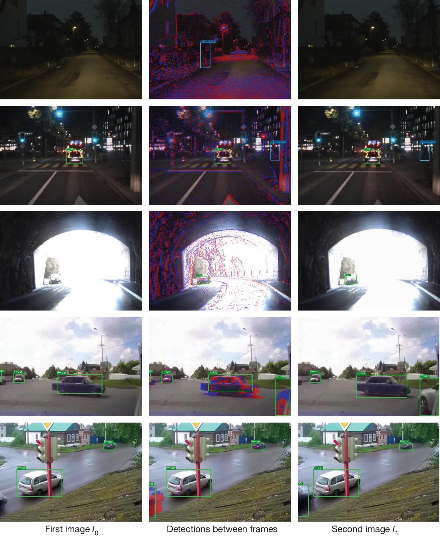
Thermal imaging sensors offer unparalleled versatility, capable of detecting heat differences in total darkness, measuring temperature, and identifying distant objects. They are particularly well suited for a wide range of surveillance applications, especially in challenging and life-saving scenarios. Compared to prevailing thermal sensor solutions, which typically suffer from low resolution, high cost, and limited production volumes, Obsidian is revolutionizing the thermal imaging industry by producing high resolution thermal sensors with its proprietary Large Area MEMS Platform (“LAMP”), offering low-cost production at high volumes. With large glass substrates capable of producing sensors with superior resolution, VGA or higher, at volumes exceeding 100 million units per year, Obsidian is poised to drive the mass market adoption of this unrivaled technology across industries, including automotive, security, surveillance, drones, and more.

With accelerating interest in both the consumer and defense sectors, Obsidian’s groundbreaking thermal imaging sensor solutions are gaining traction in automotive applications and poised to play a pivotal role. The novel ADAS (Advanced Driver Assistance Systems) and AEB (Automatic Emergency Braking) system, integrated with Obsidian’s thermal sensors, significantly enable higher-resolution and clear vision in low-light and adverse weather conditions such as fog, smoke, rain, and snow, ensuring much better driving safety and security. This aligns perfectly with measures announced by the NHTSA (National Highway Traffic Safety Administration) on April 29, 2024, which issued its final rule mandating the implementation of AEB, including PAEB (Pedestrian AEB) that is effective at night, as a standard feature on all new cars beginning in 2029, recognizing pedestrian safety features as essential components rather than just luxury add-ons. This safety standard is expected to significantly reduce rear-end and pedestrian crashes. Traffic safety authorities in other countries are also following suit with similar regulations underscoring the trend and significant potential demand for thermal imaging sensors from Obsidian Sensors in the years to come.


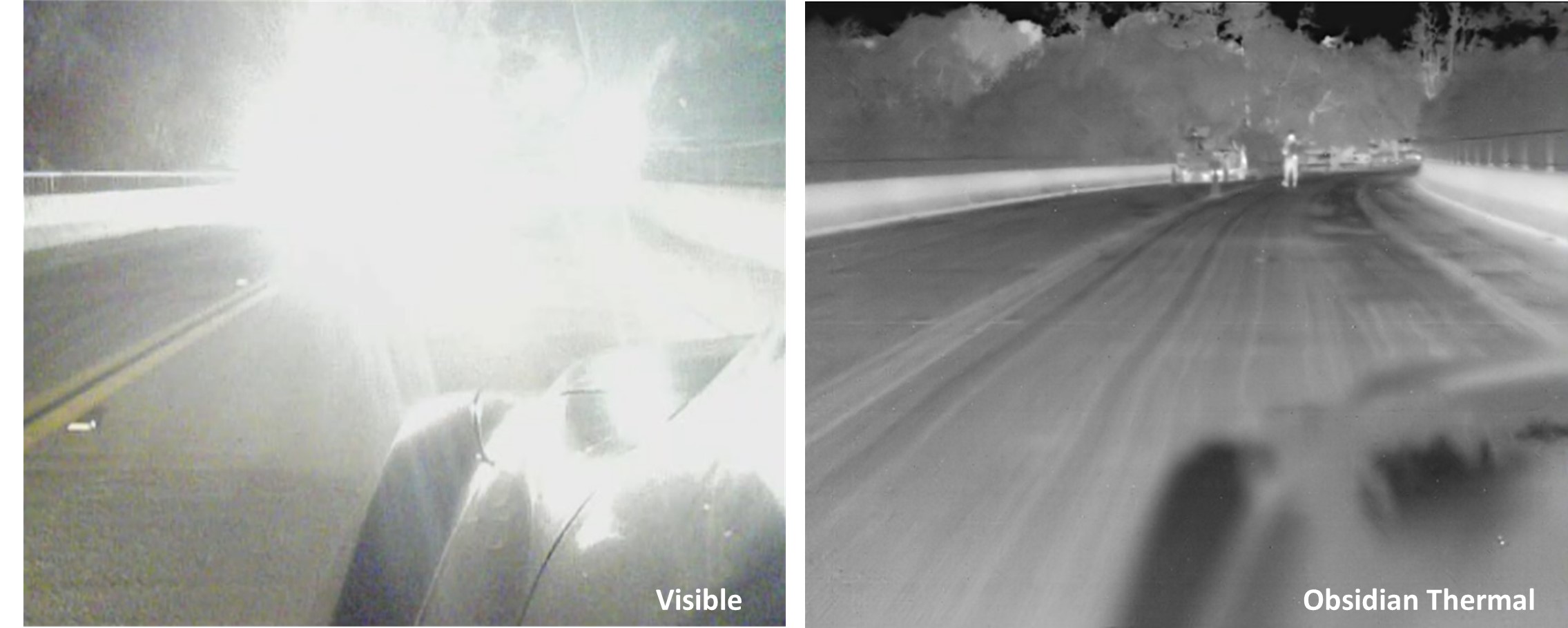
A dangerous nighttime driving situation can be averted with a thermal camera
 

“We are pleased to begin our strategic partnership with Himax through this funding round and look forward to a fruitful collaboration to potentially merge our market leading thermal imaging sensor and camera technologies with Himax’s advanced ultralow power WiseEyeTM endpoint AI, leveraging each other's domain expertise. Furthermore, progress has been made in the engineering projects for mixed signal integrated circuits, leveraging Himax’s decades of experience in image processing. Given our disruptive cost and scale advantage, this partnership will enable us to better cater to the needs of the rapid-growing thermal imaging market,” said John Hong, CEO of Obsidian Sensors.

“We see great potential in Obsidian Sensors' revolutionary high-resolution thermal imaging sensor. Himax’s strategic investment in Obsidian further enhances our portfolio and expands our technology reach to cover thermal sensing which represents a great compliment to our WiseEye technology, a world leading ultralow power image sensing AI total solution. Further, we see tremendous potential of Obsidian’s technology in the automotive sector where Himax already holds a dominant position in display semiconductors. We also anticipate additional synergies through expansion of our partnership with our combined strength and respective expertise driving future success,” said Mr. Jordan Wu, President and Chief Executive Officer of Himax.

Monday, June 10, 2024

IEEE SENSORS 2024 Update from Dan McGrath


IEEE SENSORS 2024 Image Sensor Update

This is a follow-up to my earlier Image Sensor World post on how the program initiative related to image sensors participation in IEEE SENSORS 2024 is coming together. Two activities targeted at the image sensor community have been organized as follows:

·         A full-day workshop on Sunday, 20 October, organized by Sozo Yokogawa of SONY and Erez Tadmor of onSemi, titled “From Imaging to Sensing: Latest and Future Trends of CMOS Image Sensors”. It includes speakers from Omnivision, onSemi, Samsung, Canon, SONY, Artilux, TechInsights and Shizuoka University.

·         A focus session on Monday afternoon, 21 October, organized by S-G Wuu of Brillnics, DN Yang of TSMC and John McCarten of L3/Harris on stacking in image sensors. It will lead with an invited speaker. There is the opportunity for submitted presentations on any aspect of stacking. Those interested should submit an abstract to me at dmcgrath@ieee.org before 30 June. The selection process will be handled separately from the regular process for the conference.

This initiative is to encourage the image sensor community to give SENSORS the chance to prove itself a vibrant, interesting and welcoming home for the exchange of technical advances. It is part of the IEEE Sensors Council’s initiative to increase industrial participation across the council’s activities. Other events planned at SENSORS 2024 as part of this initiative are a session on standards and a full-day in-conference workshop on the human-machine interface. There will also be the opportunity for networking between industry and students.

Consider joining the Sensors Council – it is free if you are an IEEE member. Consider the mutual benefit of being in an organization and participating in a conference that shares more than just the name “sensors”. Our image sensor community is a leader in tackling the problems of capturing what goes on in the physical world, but there are also things that can be learned by our community from the cutting-edge work related to other sensors.

The submission date for the conference in general is at present 11 June, but there is a proposal to extend it to 25 June. Check the website.

Looking forward to seeing you in Kobe.

Dan McGrath

TechInsights Inc.

Industrial Co-Chair, IEEE SENSORS 2024

AdCom member, IEEE Solid State Circuits Society & IEEE Sensor Council

dmcgrath@ieee.org

Sunday, June 09, 2024

Conference List - September 2024

IEEE International Conference on Multisensor Fusion and Integration - 4-6 Sep 2024 - Pilsen, Czechia - Website

IEEE Sensors in Spotlight 2024 - 5 Sep 2024 - Boston, Massachusetts, USA - Website

Semi MEMS and Sensors Executive Conference - 7-9 Sep 2024 - Quebec, QC, Canada - Website

Sensor China Expo & Conference 2024 - 11-13 Sep 2024 - Shanghai, China - Website

SPIE Sensors + Imaging 2024 - 16-19 Sep 2024 - Edinburgh, Scotland, UK - Website

SPIE Photonics Industry Summit - 25 Sep 2024 - Washington, DC, USA - Website

21st International Conference on IC Design and Technology - 25-27 Sep 2024 - Singapore- Website

10th International Conference on Sensors and Electronic Instrumentation Advances - 25-27 Sep 2024 - Ibiza, Spain - Website

If you know about additional local conferences, please add them as comments.

Return to Conference List index

Wednesday, June 05, 2024

ID Quauntique webinar: single photon detectors for quantum tech


In this webinar replay, we first explore the role of single-photon detectors in advancing quantum technologies, with a focus on superconducting nanowire detectors (SNSPDs) and the benefits they offer for quantum computing and high-speed quantum communication.

After which, we discuss the evolving needs of the field and describe IDQ’s user-focused detector solutions, including our innovative photon-number-resolving (PNR) SNSPDs and our new rack-mountable SNSPD system. We show real-world experiments that have already benefited from the outstanding performances of our detectors, including an enhanced heralded single-photon source and high key-rate QKD implementation.

Finally, we conclude with our vision on the future of single-photon detection for quantum information and networking, and the exciting possibilities this can unlock.

Tuesday, June 04, 2024

ISSW 2024 this week in Trento, Italy

The 2024 International SPAD Sensor Workshop is happening this week in Trento, Italy. Full program is available here: https://issw2024.fbk.eu/program

Talks:


Posters: