Monday, August 31, 2020

Workshop on Emerging Solutions for Imaging Devices, Circuits, and Systems

ESSCIRC and ESSDERC conferences host a 6 hour-long on-line Workshop on Emerging Solutions for Imaging Devices, Circuits, and Systems chaired by Matteo Perenzoni (FBK) and Albert Theuwissen (Harvest Imaging). The program includes:

  • Applications of single photon detection in computational and quantum imaging.
    Daniele Faccio (University of Glasgow, UK)
  • Infrared detectors in the wake of visible sensors
    Patrick Robert (Lynred, France)
  • Event cameras
    Tobi Delbruck (University of Zurich, Switzerland)
  • Broadband image sensors based on 2D materials, integrated with silicon technology
    Frank Koppens (ICFO Barcelona, Spain)
  • Vertical Deep Trench MOS Capacitance principle and application to CMOS Image Sensors
    François Roy (ST Microelectronics, France)
  • Coded-exposure-pixel Image Sensors for Computational Photography
    Roman Genov (University of Toronto, Canada)

The presentations will be available online on-demand starting from September 7, 2020.

Sunday, August 30, 2020

Mediatek Creates AI that Creates Image Sensor Noise

Axiv.org paper "Learning Camera-Aware Noise Models" by Ke-Chi Chang, Ren Wang, Hung-Jin Lin, Yu-Lun Liu, Chia-Ping Chen, Yu-Lin Chang, and Hwann-Tzong Chen from Mediatek and National Tsing Hua University, Taiwan, automates image sensor model building:

"Modeling imaging sensor noise is a fundamental problem for image processing and computer vision applications. While most previous works adopt statistical noise models, real-world noise is far more complicated and beyond what these models can describe. To tackle this issue, we propose a data-driven approach, where a generative noise model is learned from real-world noise. The proposed noise model is camera-aware, that is, different noise characteristics of different camera sensors can be learned simultaneously, and a single learned noise model can generate different noise for different camera sensors. Experimental results show that our method quantitatively and qualitatively outperforms existing statistical noise models and learning-based methods."

Saturday, August 29, 2020

Photonis Demos Color Night Imaging at 0.01 Lux

Photonis publishes a demo of its Nocturn color camera at 0.01 Lux scene illumination.

"The NOCTURN Color models are powered by the proprietary KAMELEON imaging sensor, a solid-state sensor that offers less than 4e- read noise, with SXGA (1280×1024) resolution at frame rates up to 100 Hz. The KAMELEON sensor provides large 9.72µm pixels with microlenses for optimum quantum efficiency in excess of 60%, providing high-resolution low light color images that extend the vision of the human eye."


Friday, August 28, 2020

Microbolometric Technology Review

Nanjing University, China, publishes and MPDI review paper "Low-Cost Microbolometer Type Infrared Detectors" by Le Yu, Yaozu Guo, Haoyu Zhu, Mingcheng Luo, Ping Han, and Xiaoli Ji. The review belongs to "Miniaturized Silicon Photodetectors: New Perspectives and Applications" special issue.

"The complementary metal oxide semiconductor (CMOS) microbolometer technology provides a low-cost approach for the long-wave infrared (LWIR) imaging applications. The fabrication of the CMOS-compatible microbolometer infrared focal plane arrays (IRFPAs) is based on the combination of the standard CMOS process and simple post-CMOS micro-electro-mechanical system (MEMS) process. With the technological development, the performance of the commercialized CMOS-compatible microbolometers shows only a small gap with that of the mainstream ones. This paper reviews the basics and recent advances of the CMOS-compatible microbolometer IRFPAs in the aspects of the pixel structure, the read-out integrated circuit (ROIC), the focal plane array, and the vacuum packaging."

One interesting type of microbolometer is based on forward-biased SOI diodes:

"The typical value of the sensitivity for a single diode at 300 K is ~2 mV/K under a bias voltage of 0.6 V [59], which is equivalent to a temperature coefficient of only ~0.33%/K. However, as the number of the diodes in the series increases, the temperature coefficient could become comparable to the TCR of VOx. For instance, when n = 8, the diodes in series connection have a temperature coefficient of ~3%/K. Meanwhile, benefiting from the high uniformity of the CMOS process and the low defect density in the SOI film, the diode type microbolometer usually exhibits much better noise."

Xiaomi Demos 3rd Generation Under-Display Camera

Xiaomi publishes a Youtube video showing its 3rd generation under-display camera. The company expects to put it in a mass production phone next year:


GizmoChina reports that the 1st and 2nd generation used OLED displays with reduced pixel density in the camera area. The 3rd generation uses the same OLED pixel pitch, but the OLED "fill factor" is reduced to that light can penetrate to the camera. That way, pixel density, color accuracy, color gamut, and brightness in the camera area is similar to the rest of the display.


SparrowsNews adds few more details and links to the Chinese sources:

Thursday, August 27, 2020

Senseeker Introduces Oxygen DROIC Quarter Wafers

Senseeker Engineering introduces quarter wafers of the Oxygen RD0092 digital readout IC (DROIC). This allows customers to acquire a reduced minimum order quantity of ICs at lower-cost for evaluation and prototyping.

Each fully tested quarter wafer is supplied with a minimum number of guaranteed good die. A full data pack that includes a GUI-based clickable wafer map is also furnished. The wafer map provides color-coded grade information for each die along with a top-level summary (die yield, results of each individual test, and final grade). Clicking any die on the map displays a detailed test summary plot that contains test images, histograms for the test images, pixelwise differences used to reject bad pixels with pass/fail thresholds indicated, bad pixel map image and a bar graph showing the measured supply currents in the screen test state.

To further simplify the evaluation and development experience using the Oxygen RD0092, Senseeker offers an evaluation kit that can be used for cooled or uncooled lab testing. The evaluation kit comes complete with software and is easily connected to a host PC with a frame grabber card for image display.

"We are focused on making it as inexpensive and easy as possible for customers to get up-and-running with Senseeker's commercial readout products," said Kenton Veeder, President at Senseeker Engineering. "Our goal is to lower the barriers-to-entry of using advanced digital readout ICs by making them available off-the-shelf in lower quantities than a full wafer. We also believe that it is critical to provide the whole ecosystem of tools that are required to expedite the development process."


Yole Talks about Massive Drop of LiDAR Prices

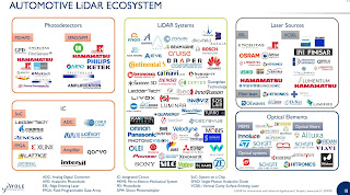
Yole Developpement 1, Yole Developpement 2: “The price drop in LiDAR in the past three years has been massive,” says Pierrick Boulay, Technology & Market Analyst, Solid-state Lighting at Yole Développement (Yole). “Indeed, it is the result of strategies by different companies and not due to the result of mass-production. Volumes have not evolved significantly in these three years and mass adoption of LiDAR still has to happen. However, this price drop of LiDAR has a significant impact on market forecast. At Yole, we expect that the unit price of LiDAR will continue to decline, and large volumes will be needed in order to maintain the market.

"A new trend in the LiDAR business appeared a few years ago, which might dramatically change the shape of LiDAR market, namely price drops. Velodyne has announced a plan to reach an average unit price of $600 by 2024, from $17,900 in 2017. Chinese LiDAR companies, which usually have LiDAR unit prices one-fifth of other companies and usually below $1,000, are gaining market share and expanding their business. LiDAR with lower unit prices is expected to enter new industrial applications including factory, logistics and security. However, because of lower LiDAR unit prices, the industrial segment is expected to have moderate growth between 2019 and 2025, expanding from $390M to $567M."

Hole Area Clarity Achievement

BusinessWire, The Elec: Samsung Display announced today that UL has just verified its new smartphone OLED hole display area as having image quality low in color deviation in terms of “hole area clarity.”

Enabling uniform image quality on the display at the periphery of the camera hole allows users to feel a more in-depth sense of picture-taking immersion, in addition to directly benefiting from the ingenuity of the hole design itself,” said Dennis Choi, VP of mobile display marketing team for Samsung Display. “Without a doubt, our camera hole area clarity demonstrates that Samsung Display technological prowess can deliver optimal performance across an entire 5G smartphone display.

Wednesday, August 26, 2020

Introduction to cwToF from Melexis

Melexis publishes a webinar on continuous wave ToF sensors:


The company also publishes another ToF video demoing its in-cabin monitoring:


Melexis also has a special Youtube channel dedicated to ToF imaging.

More about TSMC CIS Roadmap

Few more slides from TSMC Technology Symposium 2020 have been published at moore.live site. TSMC aims its 28nm CIS process to shrinking the pixel pitch from the current state of the art of 0.8um to 0.7um:


The next generation stacking process includes a fairly recent 12nm FinFET process for the bottom logic wafer:


Talking about the 12nm process intended use cases, TSMC mentions: "TSMC developed N12e specifically for AI-enabled IOT and other high efficiency, high performance edge devices. N12e brings TSMC’s world class FinFET transistor technology to IOT.

...Enhanced Machine Vision – insects, shadows or animals often falsely trigger connected security cameras. By moving the image classifier to the edge, the AI-enabled connected cameras can continually monitor for humans – even with facial recognition but ignore pets and insects without sending gigabytes of HD video into the cloud for inferencing.
"

ON Semi on Surround Camera Trends

ON Semi publishes a webinar recording on automotive surround view cameras:

Tuesday, August 25, 2020

TSMC Updates on CIS Process Development

AnandTech: TSMC Technology Symposium being held on-line these days shows the foundry's lineup of the processes. The most advanced CIS process in development is 28nm, while the logic process is 7 generations ahead at 3nm:


TodayUSStock posts few more slides form the Symposium:

Omnivision Moves 2MP Sensor Production to 12" Wafers

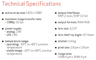
BusinessWire: OmniVision announces the OS02G10 1080p30 security sensor with a 2.8um OmniPixel3-HS architecture. Compared with OmniVision’s prior-generation mainstream security sensor, it has a 60% better SNR1 and 40% lower power consumption.

OmniVision is using 12” wafers to produce this image sensor, instead of the 8” wafers that are in tight supply but are typically used for 2MP, 1080p sensors. This enables the company to better address the increasing demand for this resolution, which remains the most popular in the steadily growing market for consumer-grade, IoT security cameras, as well as low-end industrial and commercial surveillance cameras.

The OS02G10 builds on the success of our previous-generation OmniPixel 3-HS sensor, which has been widely adopted in the mainstream security markets,” said Cheney Zhang, senior marketing manager for the security segment at OmniVision. “With this new generation, we have significantly improved low-light performance while continuing to offer the market greater value in the popular 1/2.9” optical format.

Monday, August 24, 2020

Luminar Goes Public Through Reverse Merger at $3.4B Valuation

BusinessWire: After Velodyne, another LiDAR company, Luminar, goes public on NASDAQ by reverse merging with Gores Metropoulos. The transaction includes $400M of cash from Gores Metropoulos and an immediate $170M financing into Luminar. The combined company will have an implied pro forma enterprise value of approximately $2.9 billion and an equity value of approximately $3.4 billion at closing.

"Founded in 2012 by CEO Austin Russell, Luminar is the leading autonomous vehicle and lidar technology company for consumer cars and trucking. Luminar is partnered with 7 of the top 10 global automakers and is set to power the introduction of highway self-driving and next-generation safety systems. Over 350 people strong, Luminar has built a new type of lidar from the chip-level up with breakthroughs across all core components.

Luminar today also announced it has scaled its software team with the addition of 16 former members of Samsung’s Munich-based DRVLINE platform team that were previously responsible for delivering ADAS functionality to its mobility customers. Luminar will leverage this team to bring a full-stack lidar-based ADAS and Level 4 highway autonomy product offering to market.
"

Luminar's presentation talks about the company's achievements:


Like in case of Velodyne, becoming a public company gives us a rare opportunity to look into the LiDAR company economics:

VivaMOS Receives £4.8M Funding for Low-Noise Wafer-Scale X-Ray Sensor

EENews: vivaMOS receives £4.8M (€5.3M) grant to develop an ultra-low noise X-Ray wafer scale sensor for optical astronomy and medical imaging. vivaMOS, based in Southampton, UK, spun out of the Rutherford Appleton laboratory in 2015 to commercialize the 6.7MP wafer-scale Lassena X-ray image sensor.

We’ve been involved in several other projects detecting signals from very low radiation sources. Although these have resolved information to a promising level, they’re not quite there yet,” said Dan Cathie, CEO at vivaMOS. “We know the sensor is best-in-class on noise performance and have committed to pursuing it further to see if a product can be developed through this SPRINT ultra-low noise optical astronomy project."

VivaMOS presentation in CERN in 2019 discloses some parameters of the company's Lassena sensor:


Thanks to MN for the link!

Sunday, August 23, 2020

ADI Proposes ToF Baby Monitor Camera, Compares cwToF and pToF Approaches

Arrow and Analog Devices propose to use its ToF camera solution in baby monitors:


ADI also publishes a nice article dated by Dec 2019 and summarizing the company's experience with continuous wave and pulsed ToF systems:

Advantages of Continuous-Wave Systems:
  • For applications that do not have high precision requirements, a CW system may be easier to implement than a pulse-based system in that the light source does not have to be extremely short, with fast rising/falling edges, though it is difficult to reproduce a perfect sinusoidal wave in practice. However, if precision requirements become more stringent, higher frequency modulation signals will become necessary and may be difficult to implement in practice.
  • Due to the periodicity of the illumination signal, any phase measurement from a CW system measurement will wrap around every 2π, meaning that there will be an aliasing distance. For a system with only one modulation frequency, the aliasing distance will also be the maximum measurable distance. To counteract this limitation, multiple modulation frequencies can be used to perform phase unwrapping, wherein the true distance of an object can be determined if two (or more) phase measurements with different modulation frequencies agree on the estimated distance. This multiple modulation frequency scheme can also be useful in reducing multipath error, which occurs when the reflected light from an object hits another object (or reflects internally within the lens) before returning to the sensor, resulting in measurement errors.
  • Depending on their configuration, CMOS ToF imagers tend to have more flexibility and faster readout speed, so functions such as region-of-interest (RoI) output are possible.
  • Calibrating a CW ToF system over temperature may be easier than that of a pulsed ToF system. As the temperature of a system increases, the demodulation signal and the illumination will shift with respect to each other because of the temperature variation, but this shift will only affect the measured distance with an offset error that is constant over the entire range, with the depth linearity remaining essentially stable.

Disadvantages of Continuous-Wave Systems:
  • Though CMOS sensors have higher output data rates compared to that of other sensors, CW sensors require four samples of the correlation function at multiple modulation frequencies, as well as multiframe processing, to calculate depth. The longer exposure time can potentially limit the overall frame rate of the system, or can cause motion blur, which can limit its use to certain types of applications. This higher processing complexity can necessitate an external application processor, which may be beyond the application’s requirements.
  • For longer distance measurements or environments with high levels of ambient light, higher continuous optical power (compared to that of pulsed ToF) will become necessary; this continuous illumination from the laser could cause thermal and reliability issues.

Advantages of Pulse-Based ToF Technology Systems:
  • Pulse-based ToF technology systems often rely on high energy light pulses emitted in very short bursts during a short integration window. This offers the following advantages:
  • It makes it easier to design a system that is robust to ambient light, therefore more conducive to outdoor applications.
  • The shorter exposure time minimizes the effect of motion blur.
  • The duty cycle of the illumination in a pulse-based ToF system is generally much lower than that of a comparable CW system, thereby offering the following benefits:
  • It lowers the overall power dissipation of the system in longer range applications.
  • It avoids interference from other pulsed ToF systems by placing the pulse bursts in a different location in the frame from that of the other systems. This can be done by coordinating the placement of the pulses in the frame of the various systems or by using an external photodetector to determine the location of the other system’s pulses. Another method is to dynamically randomize the location of the pulse bursts, which will eliminate the need to coordinate the timing between the various systems, but it will not completely eliminate the interference.
  • Since the pulse timing and width do not need to be uniform, different timing schemes can be implemented to enable functions such as wider dynamic range and auto-exposure.

Disadvantages of Pulse-Based ToF Technology Systems:
  • Since the pulse width of the transmitted light pulse and the shutter need to be the same, the timing control of the system needs to be highly precise, and a picosecond level of precision may be required depending on the application.
  • For maximum efficiency, the illumination pulse width needs to be very short, but with very high power. For this reason, very fast rising/falling edges (less than 1 ns) are required from the laser driver.
  • Temperature calibration may be more complicated, compared to that of CW systems since a variation in temperature will affect individual pulse widths, affecting not only the offset and gain, but also its linearity.

Saturday, August 22, 2020

Dahua Cameras with Sony Starvis Sensors Provide Color Night Vision Down to 0.004 lux

Businesswire: Dahua’s flagship Starlight technology employs large apertures (maximum f/1.6), Sony Starvis sensors and Smart ISP to produce richly colored, identification-level images in illumination of 0.004 to 0.009 lux. Starlight cameras have IR cut filters that switch to black and white mode when the camera senses that insufficient light is available to reproduce good color images. When night mode is triggered, the filter disengages, allowing IR as well as visible illumination to reach the image sensor.

There is also a Night Color mode that does not require a IR cut filter; instead it uses a high-performance sensor and ISP, as well as an achromatic large aperture lens, to produce crisp, clear images. Night Color requires at least 1 lux of ambient or artificial light.

TrendForce: Sanctions on Huawei Cause CIS Market Decline by Extra 0.2%

SemiconductorDigest, BusinessWire: TrendForce publishes its forecast of impact of expanded US sanctions against Huawei on five major tech industries. Regarding the CIS market, analysts say:

"TrendForce previously forecasted a 1.3% YoY revenue decline in 2020 for the CIS (CMOS image sensor) industry due to the poor sales performances of the smartphone and automotive markets, which are the primary markets for CIS applications, as a result of the COVID-19 pandemic. After the latest restrictions on Huawei by the U.S. government on August 17, TrendForce is now further increasing the forecasted decline in CIS revenue to 1.5% in consideration of Sony’s inability to ship its high-end camera modules to Huawei."

Friday, August 21, 2020

SeeDevice Announces Licensing Agreement With MegaChips

PRNewswire: SeeDevice announces a licensing agreement with MegaChips Corporation, a fabless LSI Company. The agreement allows MegaChips to integrate SeeDevice's Photon Assisted Tunneling - Photo Detector (PAT-PD) smart vision sensor into their products. So far, Megachips does not have image sensor products in its portfolio.

"This licensing agreement is a validation of our technology maturity and ability to serve a major partner and supplier like MegaChips. Our PAT-PD sensor not only outperforms existing image sensors, it helps create an entirely new category of photon sensing capability," said Hooman Dastghaib, CEO of SeeDevice. "For example, sensitivity for photo-diodes is measured in uV per electron generated, or amps/watt (A/W), and generates a relatively low responsiveness of less than 1 A/W. Our PAT-PD sensor, using quantum tunneling, can produce a variable output between 102 and 108 A/W, far surpassing the ability of today's leading CMOS image sensors, producing higher-quality images in a wider variety of lighting conditions."

PAT-PD also expands the photosensitive light range of CMOS sensors beyond visible light into NIR spectrum (between 300nm-1,600nm) with plans to increase this to 2,000nm with the next-generation of sensors, pushing into SWIR band.

Additionally, the PAT-PD sensor boosts photoelectric conversion efficiency to 1e7, while maintaining a SNR over 60dB at room temperature. Reaction time is also reduced from microseconds to sub-nanoseconds while dynamic range is boosted to 100dB linear and 150dB non-linear.

SeeDevice claims to achieve all of these results using standard CMOS fabrication process, meaning easier integration in mixed-signal process, and avoiding the use of expensive exotic materials and manufacturing processes to achieve similar results.

Quantum tunneling effect allows a photon-activated current flow to trigger using a fraction of the photons normally required in a photo-diode based design. This allows a PAT-PD sensor to trigger with just a single photon, generating a current with unprecedented efficiency and creating a signal with significantly less input over a much wider range of wavelengths. Using a PAT-PD silicon-based CMOS image sensor, devices can capture granular-level sharp details even in extremely low light conditions by utilizing infrared, near infrared, and short-wave infrared frequencies.

There are a number of additional benefits PAT-PD provides to device makers:
  • Global Shutter for CMOS Sensors
  • Higher QE
  • Higher Quality Low-Light Images
  • Higher DR

Thursday, August 20, 2020

Canon Develops 1/1.8-inch Sensor Capturing 1080p Video at 0.08Lux

Canon announces the launch in Japan of the LI7050, a new 1/1.8-inch CMOS sensor capable of capturing color images in full-HD even in low-illumination environments as dark as 0.08 lux. Despite a compact pixel array of 1/1.8 inches and pixel size of 4.1 µm, Canon’s newly developed LI7050 sensor makes possible color video recording in low-light environments as dark as 0.08 lux.

Security cameras equipped with the LI7050 can capture video at night in such locations as public facilities, roads or transport networks, thereby helping to identify details including the color of vehicles or subjects’ clothing. What’s more, this compact, high-sensitivity sensor can be installed in cameras for such use cases as underwater drones, microscopes and wearable cameras for security personnel.

Canon’s new sensor is also equipped with an HDR drive function that realizes a wide DR of 120 dB. When recording in an environment with illumination levels between, for example, 0.08 lux and 80,000 lux, the sensor’s wide dynamic range enables video capture without blown-out whites and crushed blacks. During normal drive operation, the sensor realizes a noise level of 75 dB and captures video without blown-out whites and crushed blacks in environments with illumination levels between, for example, 0.08 lux and 500 lux.
​​​​​​​
​​​​​​​Canon has begun sample shipments of the LI7050 in August, and is scheduled to officially commence sales in late October 2020.