Apple keeps filing continuation applications for its stacked pixel patent filed more than 4 years ago. The most recent continuation is named "Image Sensor Having Full Well Capacity Beyond Photodiode Capacity" by Xiaofeng Fan. The company proposes a selectable single or dual exposure control in a wafer stacked structure with per-pixel interconnects:
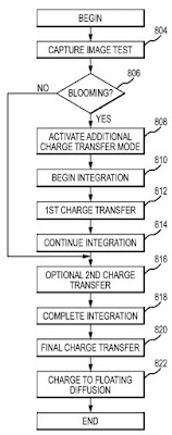
"The full well capacity of photodiodes in image sensors generally determines the exposure time, and may also affect the signal to noise ratio and/or the dynamic range of the image sensor. In some embodiments, the full well capacity of the photodiodes in the image sensor may be dynamically adjusted to allow longer exposure times, reducing blooming artifacts in captured images, and to increase the dynamic range of the image sensor. In one embodiment, the image sensor may transfer charge from the photodiode to a storage node one or more times during integration (e.g., the exposure time frame). Transferring the charge during integration may allow the full well capacity of the photodiode to be increased beyond the hardware imposed well capacity. Additionally, because the full well capacity may be varied without changing the hardware of the image sensor, the full well capacity can be dynamically varied allowing the image sensor to adjust to different lighting conditions, image capturing settings (e.g., video or still photographs), as well as allow a user to adjust the exposure time as desired without increasing blooming artifacts.
The storage node 702 may have an increased capacitance to accommodate multiple charge transfers from the photodiode 154. For example, the storage node 702 may be sufficiently large to accommodate double (or more) the capacity of the photodiode 154. This allows the storage node 702 to store charge from multiple charge transfers from the photodiode 154 as the integration time of the photodiode 154 is increased over the hardware implemented full well capacity."


This kind of ideas seems to be suitable for sub-micron pixel. However, Apple prefers to use a large pixel size. XD
ReplyDeleteLooks surprising that there should be sufficient inventive hight in applying the same principles which have already been prooven on single layer cmos imagesensors now to stacked ones for a patent. In a BSI stacked architecture FF is much less a challenge, so there is little merit in adding transistors to the puxel. But then, if your lawyers are good enough, you probably can get patented the wheel...
ReplyDeleteWith the connections between wafers being metallic...how can this work...can they fully deplete metal?
ReplyDeleteMultiple transfer or overflow from PD to SG to extend FWC was a.o. proposed by Canon, Sony, ON ...
Is it really new idea? What is the difference between this patent with DCG of Sony/Omnivision?
ReplyDeleteIsn't for example the "multiple exposure" feature of Sony Pregius G2 Sensors, e.g. IMX250 working on the same principle? Multiple transfer of charge to a charge based storage node during one integration?
ReplyDeletebtw... isnt this a global shutter pixel?
ReplyDelete