"Quantum dots are tiny (between 2 nm to 20 nm usually) semiconductor crystals. One of their unique properties is that their optical and electrical properties change with their size. In an image sensor, using quantum dots of various sizes makes it possible to capture different wavelengths of light beyond silicon’s absorption limitations. In ST’s IEDM 2021 paper, researchers tuned quantum dots to capture 940 nm and 1400 nm light, the latter rivaling InGaAs sensors. However, InGaAs imaging devices are challenging and costly to make. Using a conventional 300 mm silicon wafer process in existing fabs, ST can produce the quantum dot sensor for shortwave infrared at a fraction of the cost.
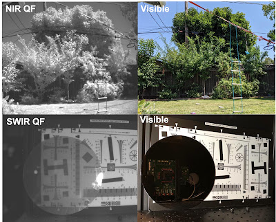
Images taken with our 940nm NIR QF sensor (top left) and with our 1400nm SWIR QF sensor (bottom left). Corresponding images taken using a visible smartphone camera (right). QF NIR image shows dramatically better contrast between black electrical wires hidden in the dark green leaves and tree trunks and branches hidden in front of the dark wood fence whereas the SWIR QF image shows how effective it is to use SWIR imaging to see through a Silicon wafer.
Quantum dots are not new, and scientists were already studying their properties in the early 1980s. However, it took years to colloidally synthesize crystals that could absorb infrared light and to create thin-film devices and fabrication processes that would yield the performance and stability necessary for real-world applications. More specifically, ST developed a manufacturing process that would not exceed 150ºC while also creating lithographic methodologies that would preserve the quantum dot’s integrity.

The IEDM 2021 paper explains in detail how ST created this image sensor technology on 300 mm wafers and describes the performance and reliability achieved to date. We plan to provide samples and evaluation kits to potential customers in 2022 and move to mass production in the coming years. Among the potential applications, mobile devices could use the new sensors to improve facial or object detection. Ultimately, a low-cost high-volume SWIR image sensor accessible to all consumers will open the door to new use-cases and applications."
What kind of sensor resolution they plan in their evaluation samples?
ReplyDelete