Press release from NIT:
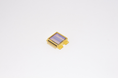
The NSC1801 line scan sensor was designed initially for imaging linearly moving objects with high frame rate, high sensitivity and low noise. Its pixel size has the world smallest size of 7.5µm that contributes the lower the manufacturing costs without increasing the cost of lenses.
Now NIT is pleased to release an updated version of NSC1801, where all key parameters have been reworked and overall performances improved. NSC1801 is currently installed in NIT Lisa SWIR cameras.
|
Features |
Benefits |
|
Pixel size 7.5x7.5µm |
Lowest pixel size in the industry to capture sharp
details |
|
Resolution 2048 pixels |
Large field of view compatible with most lenses from
the market |
|
Three gain modes available |
Allows selecting the best dynamic range for the
scene. |
|
QE >85% |
Boost sensitivity to the maximum available |
|
Line rate up to 60KHz |
For imaging fast moving objects |
|
Exposure time 10µs
to 220ms |
Fully configurable for capturing the best signal to
noise ratio |
from the package, it looks like made in China?
ReplyDeleteNot at all, it is made in France in our clean room. Pierre POTET CEO
ReplyDeleteNice Sensor, Been using for Solar cell inspection. High Res High speed.
ReplyDeletejust for curiosity... what type of inspection is done at solar cells with such kind of sensors? i mean what kind of defects can be seen at swir? e.g. cracks in silicon that get visibly due to scattering of the swir light?
DeleteHello, mainly photo emission when the solar panel is reversed biased it emits SWIR light and defective area can be easily detected . Pierre POTET
ReplyDeletethanks, very interesting, i never heard of this effect. heard of applications using the absorption of water to show for example damaged fruit, effects for plastic sorting or using the effect that silicon becomes transparent in semiconductors, but never heard of solar cells being reverse biased acting like "swir leds" for their inspection
Deletethe performance is poor
ReplyDeletepoor compare to what ?
ReplyDeleteto all we have tested
DeleteHave you tested our Line sensor ? I don't believe so since ewe have a new released version that is just sampling for now. Can you elaborate which specific performance or figure is poor ? Thank you. Pierre POTET
DeleteHow many lines?
ReplyDeleteIt is a line array so there is only one line of 2048 pixels
Delete