Infrared Colloidal Quantum Dot Image Sensors
Pejović et al. (IMEC Belgium)
Full paper: https://ieeexplore.ieee.org/document/9656610
Quantum dots (QDs) have been explored for many photonic applications, both as emitters and absorbers. Thanks to the bandgap tunability and ease of processing, they are prominent candidates to disrupt the field of imaging. This review article illustrates the state of technology for infrared image sensors based on colloidal QD absorbers. Up to now, this wavelength range has been dominated by III–V and II–VI imagers realized using flip-chip bonding. Monolithic integration of QDs with the readout chip promises to make short-wave infrared (SWIR) imaging accessible to applications that could previously not even consider this modality. Furthermore, QD sensors show already state-of-the-art figures of merit, such as sub-2- μm pixel pitch and multimegapixel resolution. External quantum efficiencies already exceed 60% at 1400 nm. With the potential to increase the spectrum into extended SWIR and even mid-wave infrared, QD imagers are a very interesting and dynamic technology segment.

Different layers in a QD image sensor

Representative images made by different QD image sensors. (a) PbS QD, SWIR image (cutoff at 1.6 μm ), 5-μm pixel pitch, and data courtesy of IMEC. (b) PbS QD, SWIR image (cutoff at 2 μm ), 15-μm pixel pitch, and data courtesy of SWIR vision systems. (c) PbS QD, SWIR image (cutoff at 2 μm ), 20-μm pixel pitch, and data courtesy of Emberion. (d) PbS QD, SWIR image (cutoff at 1.6 μm ), 2.2-μm pixel pitch, and data courtesy of STMicroelectronics. (e) PbS QD, SWIR image (cutoff at 1.85 μm ), and data courtesy of ICFO. (f) HgTe QD, MWIR image (cutoff at 5 μm ), 30-μm pixel pitch, and reprinted with permission from [51]. (g) HgTe QD, SWIR image (cutoff at 2 μm ), half VGA, 15-μm pixel pitch, and data courtesy of Sorbonne University.

Figures of Merit of Five Different PbS QD Image Sensors
Kim et al. (IMEC, Belgium)
Full paper: https://ieeexplore.ieee.org/document/9758171
Thin-film-based image sensors feature a thin-film photodiode (PD) monolithically integrated on CMOS readout circuitry. They are getting significant attention as an imaging platform for wavelengths beyond the reach of Si PDs, i.e., for photon energies lower than 1.12 eV. Among the promising candidates for converting low-energy photons to electric charge carriers, lead sulfide (PbS) colloidal quantum dot (CQD) photodetectors are particularly well suited. However, despite the dynamic research activities in the development of these thin-film-based image sensors, no in-depth study has been published on their imaging characteristics. In this work, we present an elaborate analysis of the performance of our short-wave infrared (SWIR) sensitive PbS CQD imagers, which achieve external quantum efficiency (EQE) up to 40% at the wavelength of 1450 nm. Image lag is characterized and compared with the temporal photoresponsivity of the PD. We show that blooming is suppressed because of the restricted pixel-to-pixel movement of the photo-generated charge carriers within the bottom transport layer (BTL) of the PD stack. Finally, we perform statistical analysis of the activation energy for CQD by dark current spectroscopy (DCS), which is an implementation of a well-known methodology in Si-based imagers for defect engineering to a new class of imagers.

(a) QDPD stack integration on the Si-ROIC. (b) Structure schematic of its passive PD-only device without the ROIC (ECL: edge cover layer, figures not scaled).

(a) Typical PTC for our PbS QDPD imager displaying a shot-noise-limited behavior in the relatively intense light illumination condition. (b) EQE measured with a PD-only passive device (red dashed), with an imager (black), showing no significant change in their spectral shapes and values.
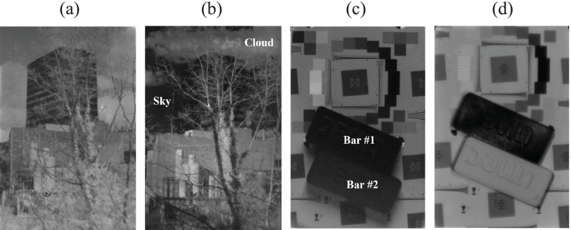
Image of the Imec campus taken with our QDPD imager on a visibly sunny day with the collection of photons in the visible spectral range [(a) < 750 nm], and in the SWIR wavelengths [(b) >1350 nm], showing bright and dark sky respectively since photons with lower energy (SWIR) are less scattered by air molecules and do not reach to the imager. Set of images capturing objects under the illumination of visible [(c) < 750 nm] and SWIR [(d) >1350 nm] light. While two plastic bars are less distinguished under visible light, they have clear contrast in the SWIR range, since the Bar #2 is more optically reflective compared with Bar #1 in that spectral region.

(a) Arrhenius plot from the PbS CQD imager pixel data (Gen 1 stack). Approximately 0.41 eV of activation energy is fitted from this plot made of median dark outputs of individual pixels. (b) Activation energy histogram computed from individual pixels, showing multiple peaks ranging from 0.23 to 0.43 eV. (c) Dark current propagation according to the temperature elevation for 0°C (left), 40°C (middle), and 80°C (right), respectively.
No comments:
Post a Comment
All comments are moderated to avoid spam and personal attacks.