Fujisaki et al. from Sony Semiconductor (Japan) presented a paper titled "A back-illuminated 6 μm SPAD depth sensor with PDE 36.5% at 940 nm via combination of dual diffraction structure and 2×2 on-chip lens" at the 2023 IEEE Symposium on VLSI Technology and Circuits.
Abstract: We present a back-illuminated 3D-stacked 6 μm single-photon avalanche diode (SPAD) sensor with very high photon detection efficiency (PDE) performance. To enhance PDE, a dual diffraction structure was combined with 2×2 on-chip lens (OCL) for the first time. A dual diffraction structure comprises a pyramid surface for diffraction (PSD) and periodic uneven structures by shallow trench for diffraction formed on the Si surface of light-facing and opposite sides, respectively. Additionally, PSD pitch and SiO 2 film thickness buried in full trench isolation were optimized. Consequently, a PDE of 36.5% was achieved at λ = 940 nm, the world’s highest value. Owing to shield ring contact, crosstalk was reduced by about half compared to a conventionally plugged one.


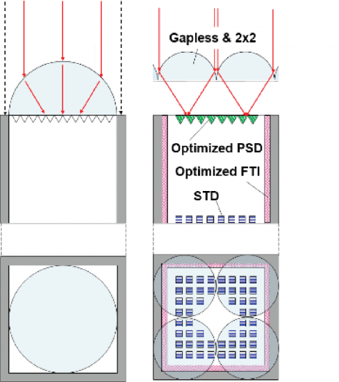
Schematics of Gapless and 2x2 on-chip lens.


Cross sectional SPAD image of (a) our previous work and (b) this work.
No comments:
Post a Comment
All comments are moderated to avoid spam and personal attacks.