In a new paper titled "Design and Characterization of 5 μm Pitch InGaAs Photodiodes Using In Situ Doping and Shallow Mesa Architecture for SWIR Sensing" Jules Tillement et al. from STMicroelectronics, U. Grenoble and CNRS Grenoble write:
Abstract: This paper presents the complete design, fabrication, and characterization of a shallow-mesa photodiode for short-wave infra-red (SWIR) sensing. We characterized and demonstrated photodiodes collecting 1.55 μm photons with a pixel pitch as small as 3 μm. For a 5 μm pixel pitch photodiode, we measured the external quantum efficiency reaching as high as 54%. With substrate removal and an ideal anti-reflective coating, we estimated the internal quantum efficiency as achieving 77% at 1.55 μm. The best measured dark current density reached 5 nA/cm2 at −0.1 V and at 23 °C. The main contributors responsible for this dark current were investigated through the study of its evolution with temperature. We also highlight the importance of passivation with a perimetric contribution analysis and the correlation between MIS capacitance characterization and dark current performance.
Full paper (open access): https://www.mdpi.com/1424-8220/23/22/9219
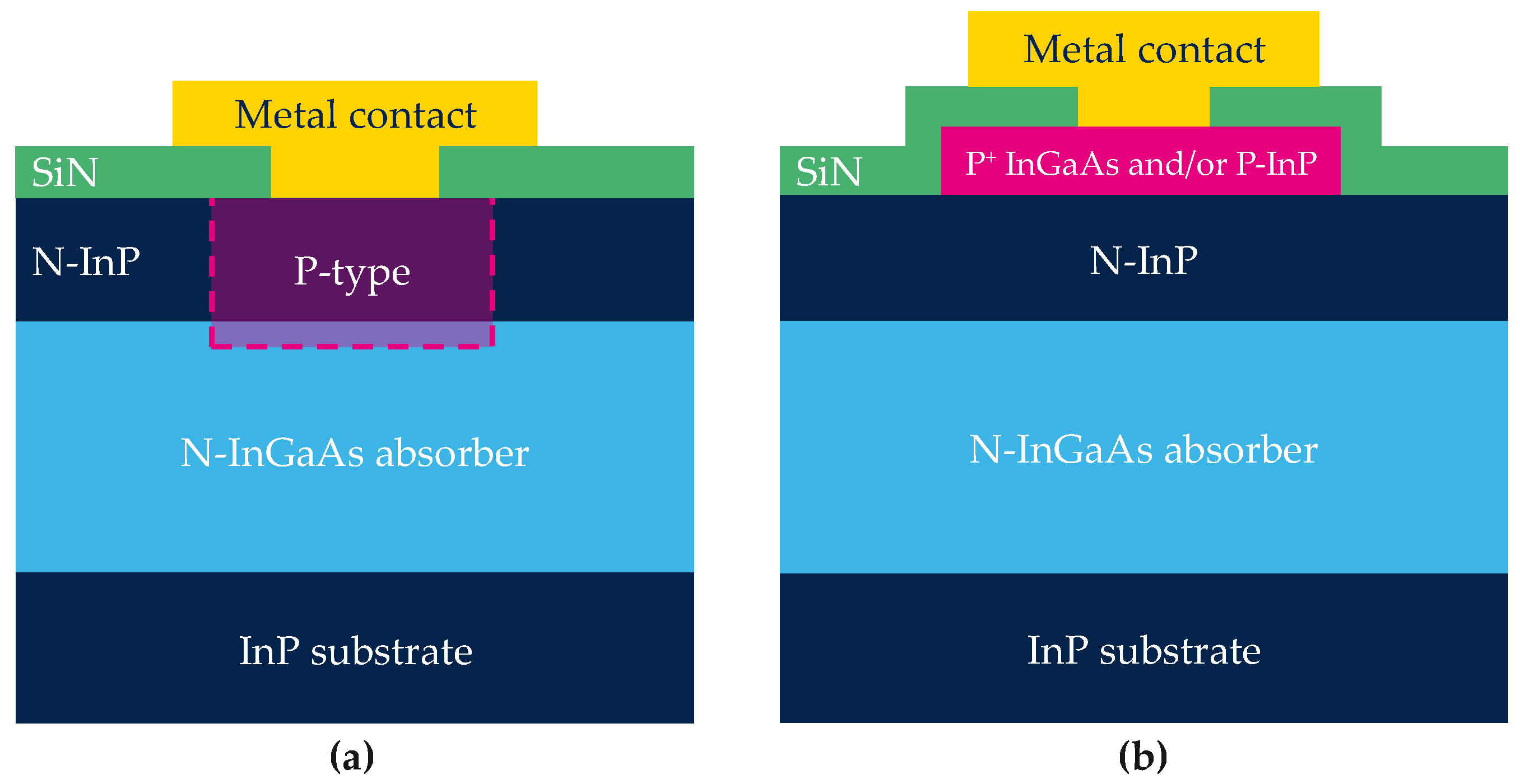
Figure 1. Schematic cross section of the photodiode after different processes. (a) Photodiode fabricated by Zn diffusion or Be implantation; (b) photodiode fabrication using shallow mesa technique.
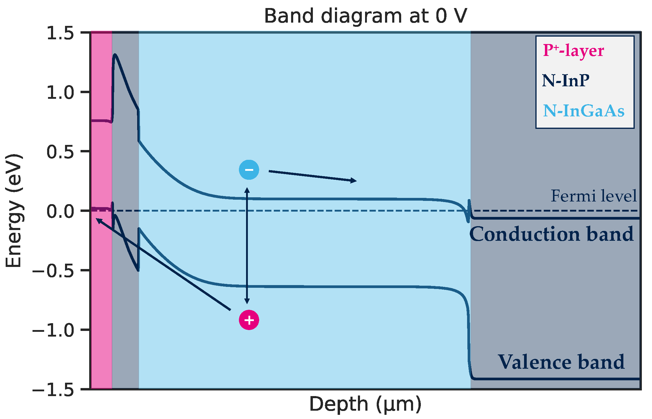
Figure 2. Band diagram of simulated structure at equilibrium with the photogenerated pair schematically represented with their path of collection.
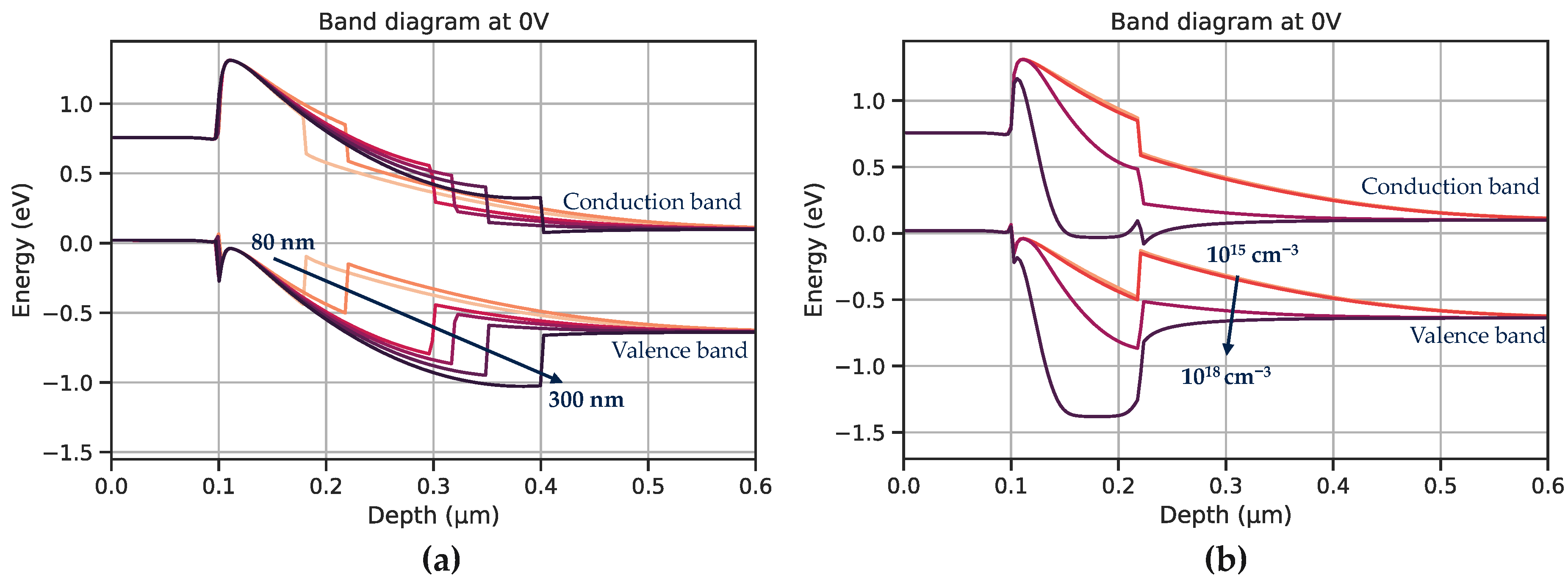
Figure 3. Top zoom of the structure—Impact of the N-InP (a) thickness and (b) doping on the band diagram at equilibrium.
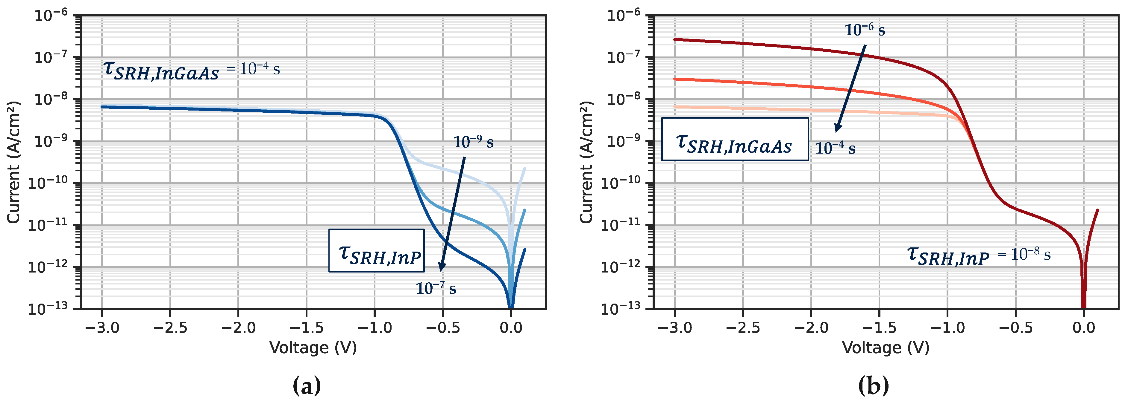
Figure 4. Simulated dark current with TCAD Synopsys tools [28]. (a) Shows evolution of the dark current when the InP SRH lifetime is modulated; (b) evolution of the dark current when the InGaAs SRH lifetime is modulated.

Figure 5. Impact of the doping concentration of the InP barrier on the carrier collection.
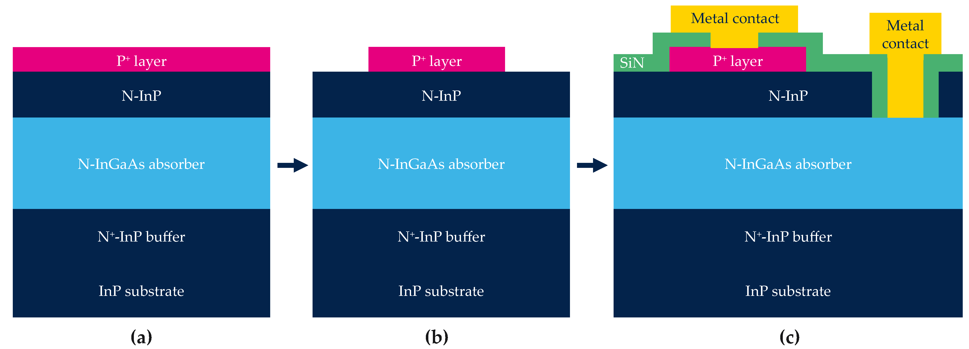
Figure 6. Simplified and schematic process flow of the shallow mesa-type process. (a) The full stack; (b) the definition of the pixel by etching the P layer and (c) the encapsulation and fabrication of contacts.
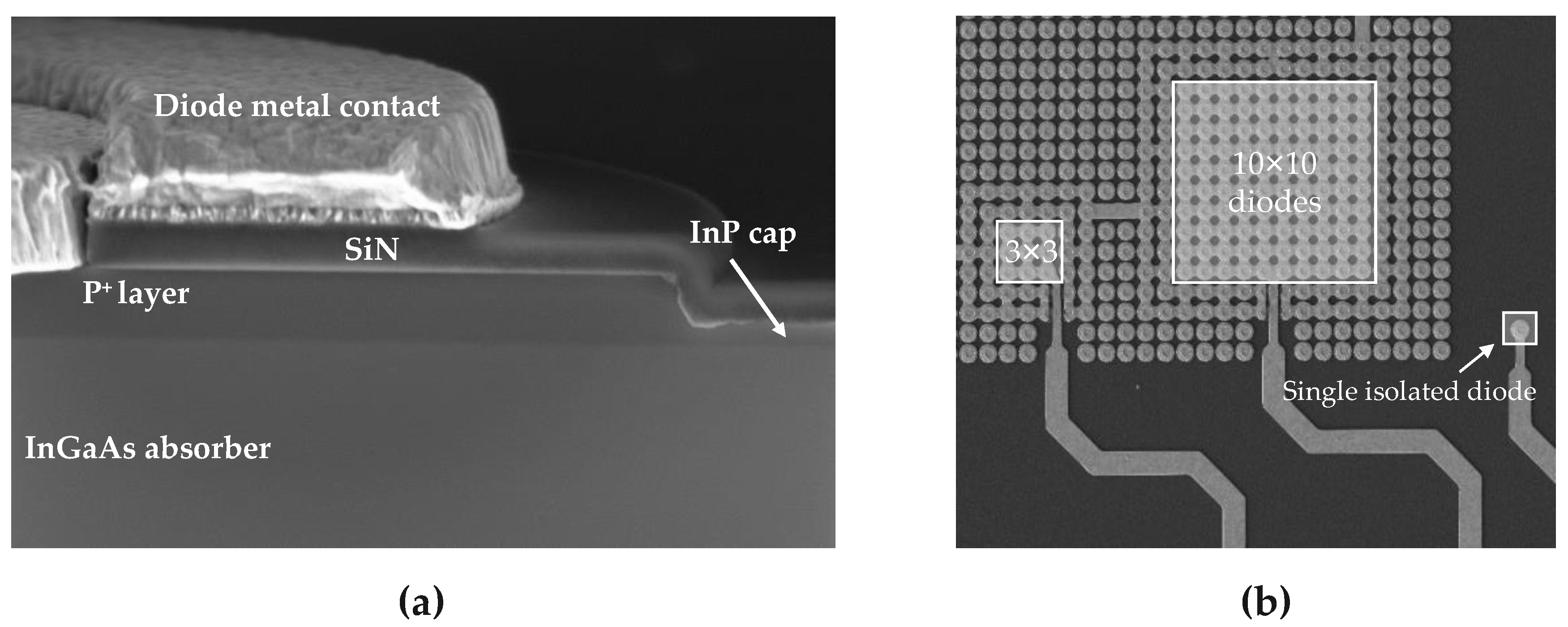
Figure 7. SEM views after the whole process. (a) A cross-section of the top stack where the P layer is etched and (b) a top view of the different configuration of the test structures (single in-array diode is not shown on this SEM view).
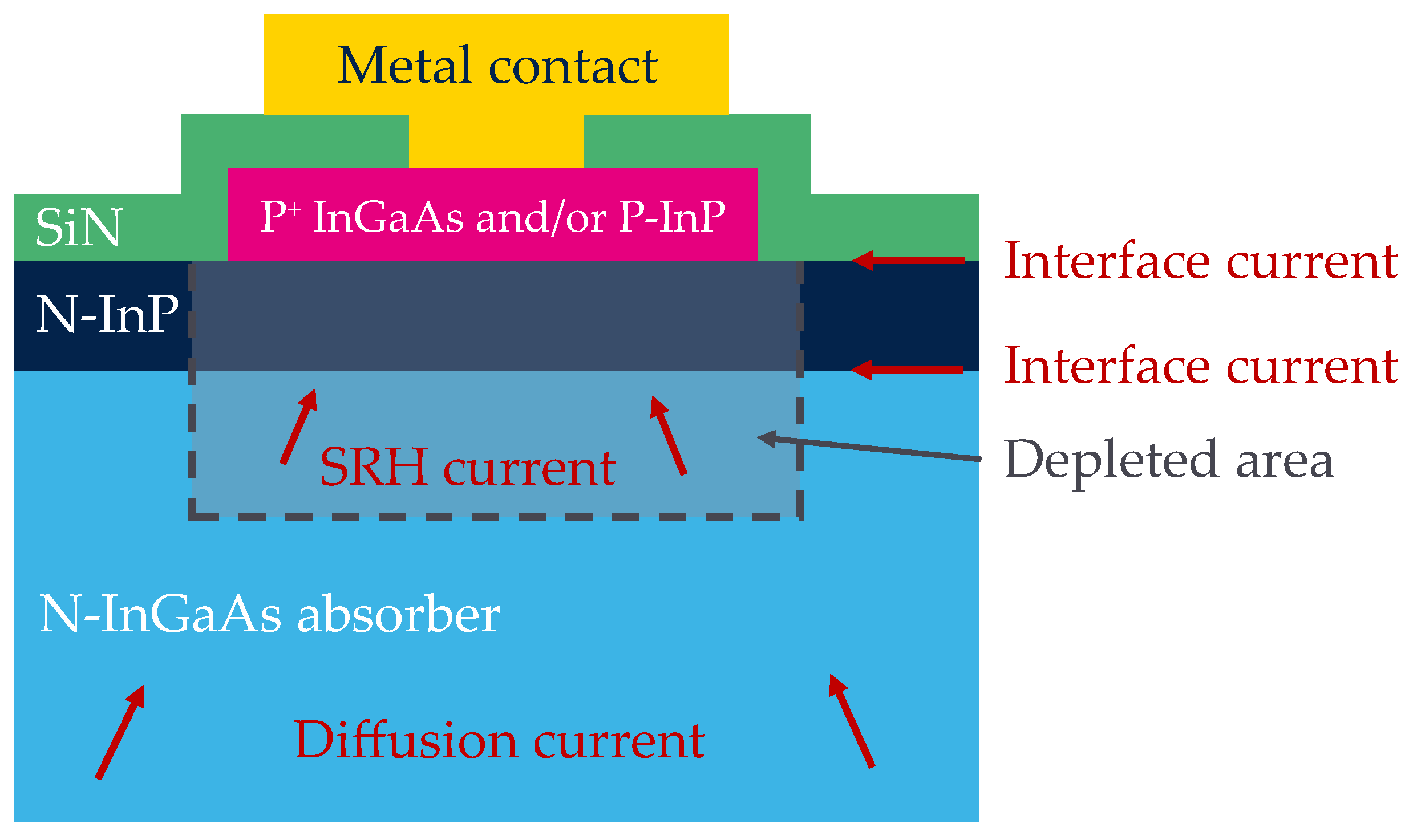
Figure 8. Schematic cross section of the structure with its potential sources of the dark current.
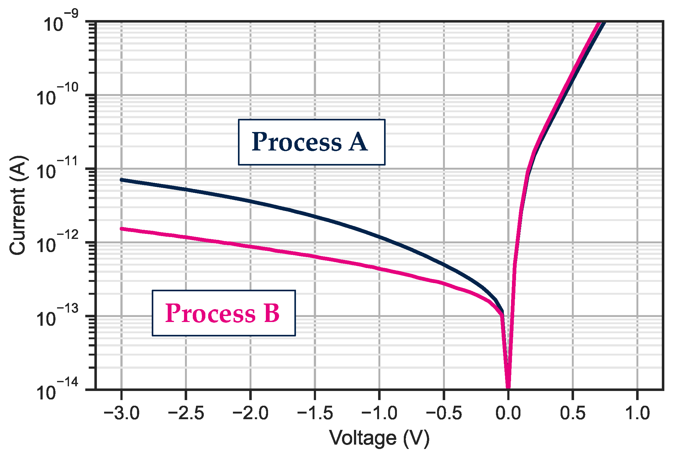
Figure 9. Dark current measurement on 15 μm pitch in a matrix like environment. The curve is the median of more than 100 single in-array diodes measured.
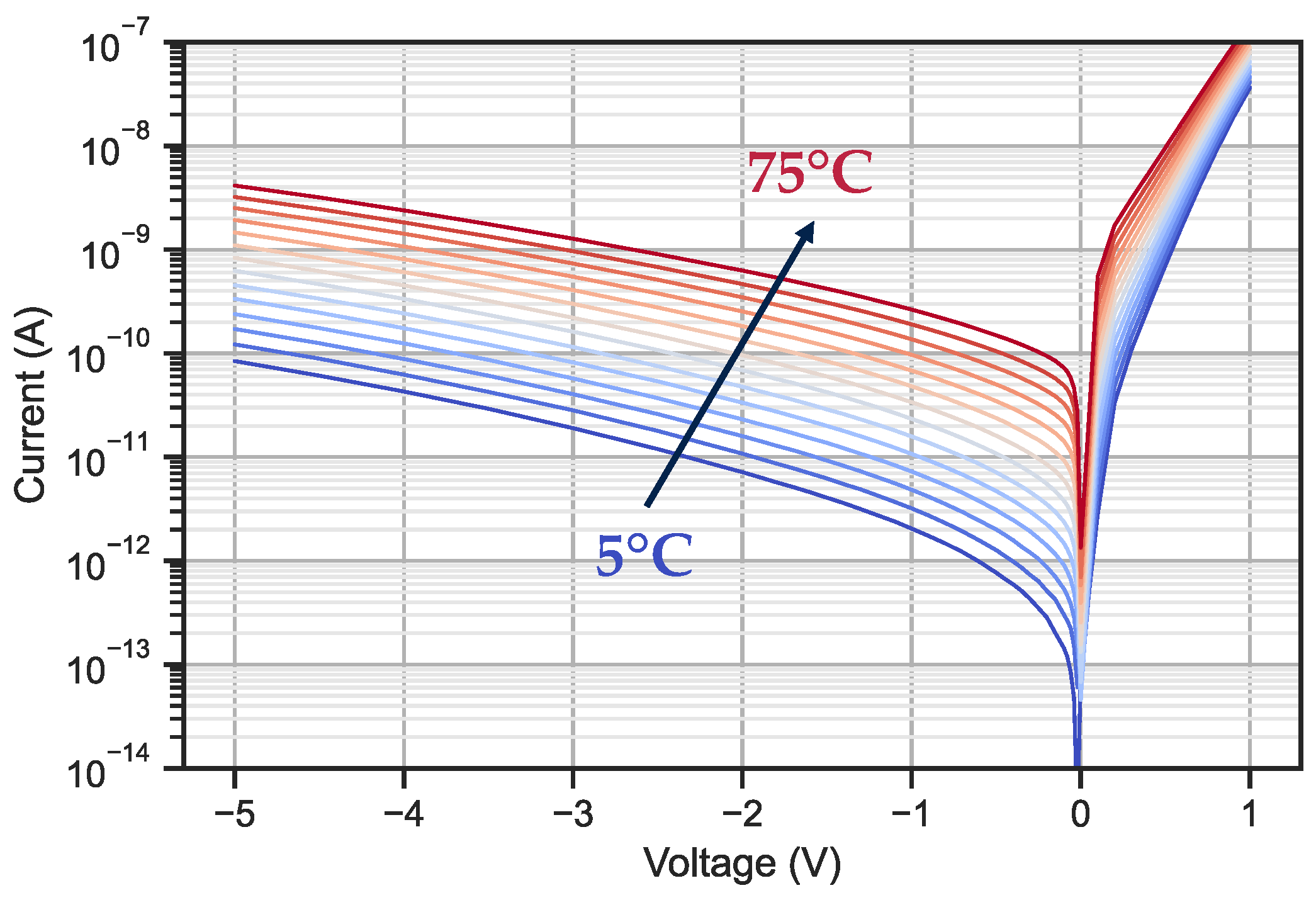
Figure 10. Dark current measurement of the ten-by-ten diode bundle. This measurement is from process B.
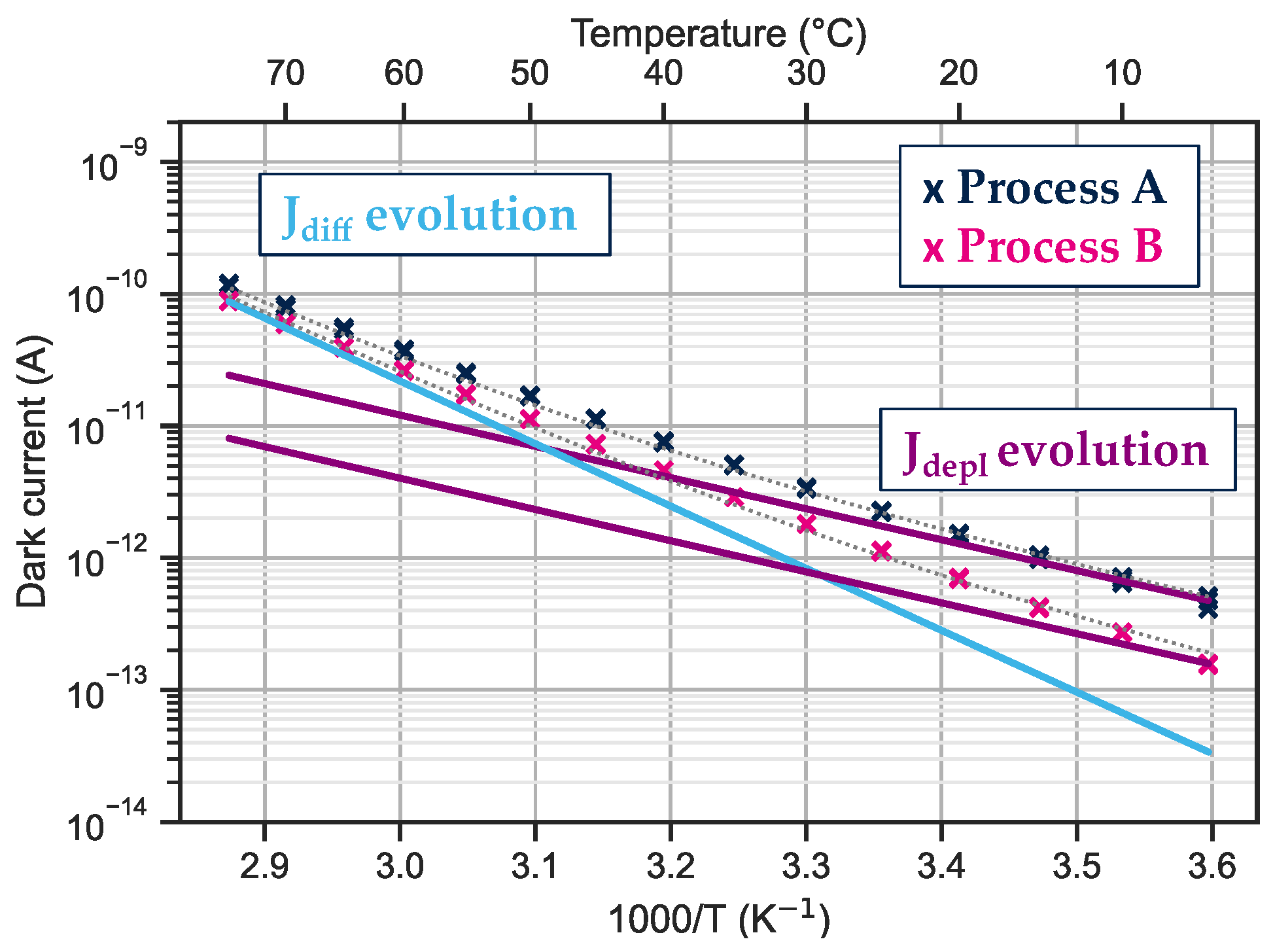
Figure 11. Evolution of the dark current with temperature at −0.1 V. The solid lines show the theoretical evolution of the current limited by diffusion (light blue line) and by generation recombination (purple line). The temperature measurement is performed on a bundle of ten-by-ten 5 μm pixel pitch diodes.
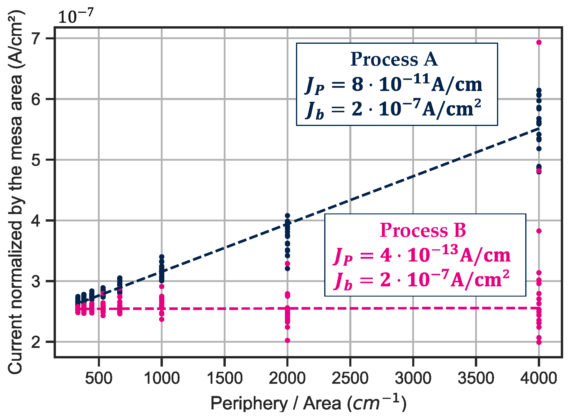
Figure 12. Perimetric and bulk contribution to the global dark current from measurements performed on diodes with diameter ranging from 10 to 120 μm.
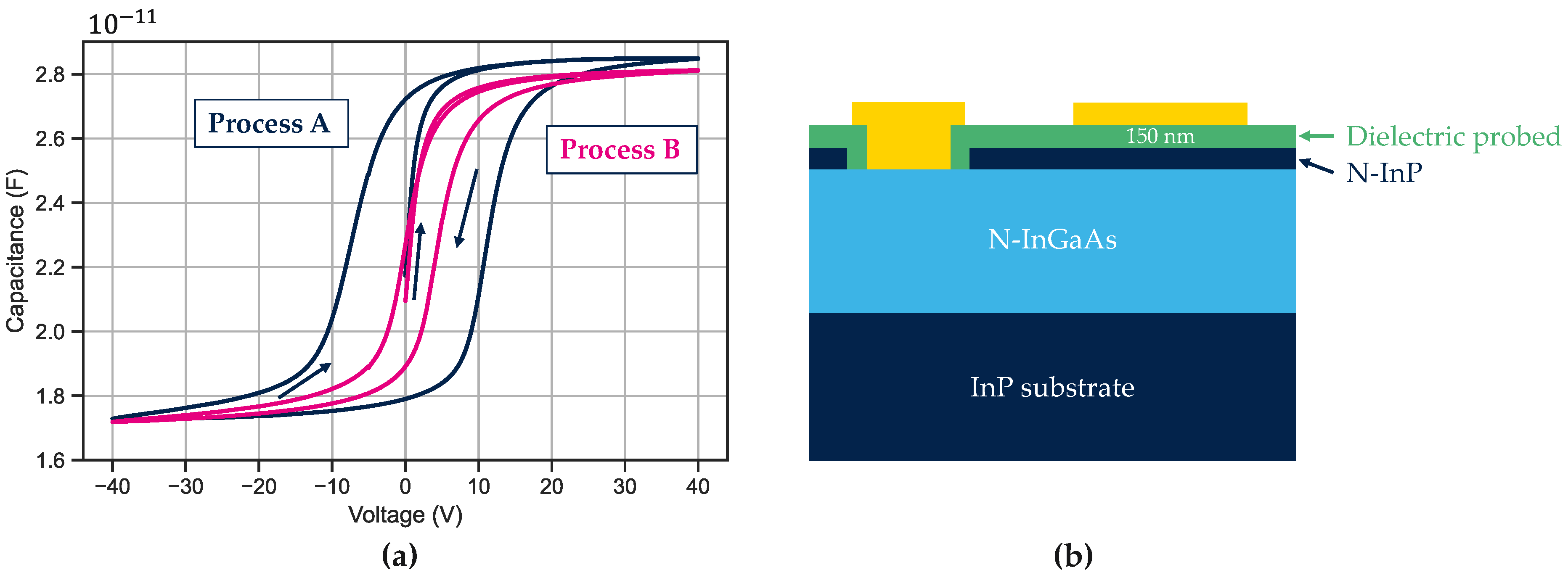
Figure 13. (a) Capacitance measurement on metal–insulator–semiconductor structure. The measurement starts at 0 V then ramps to +40 V then goes to −40 V and ends at +40 V. (b) A cross section of the MIS structure. The MIS is a 300 μm diameter circle.
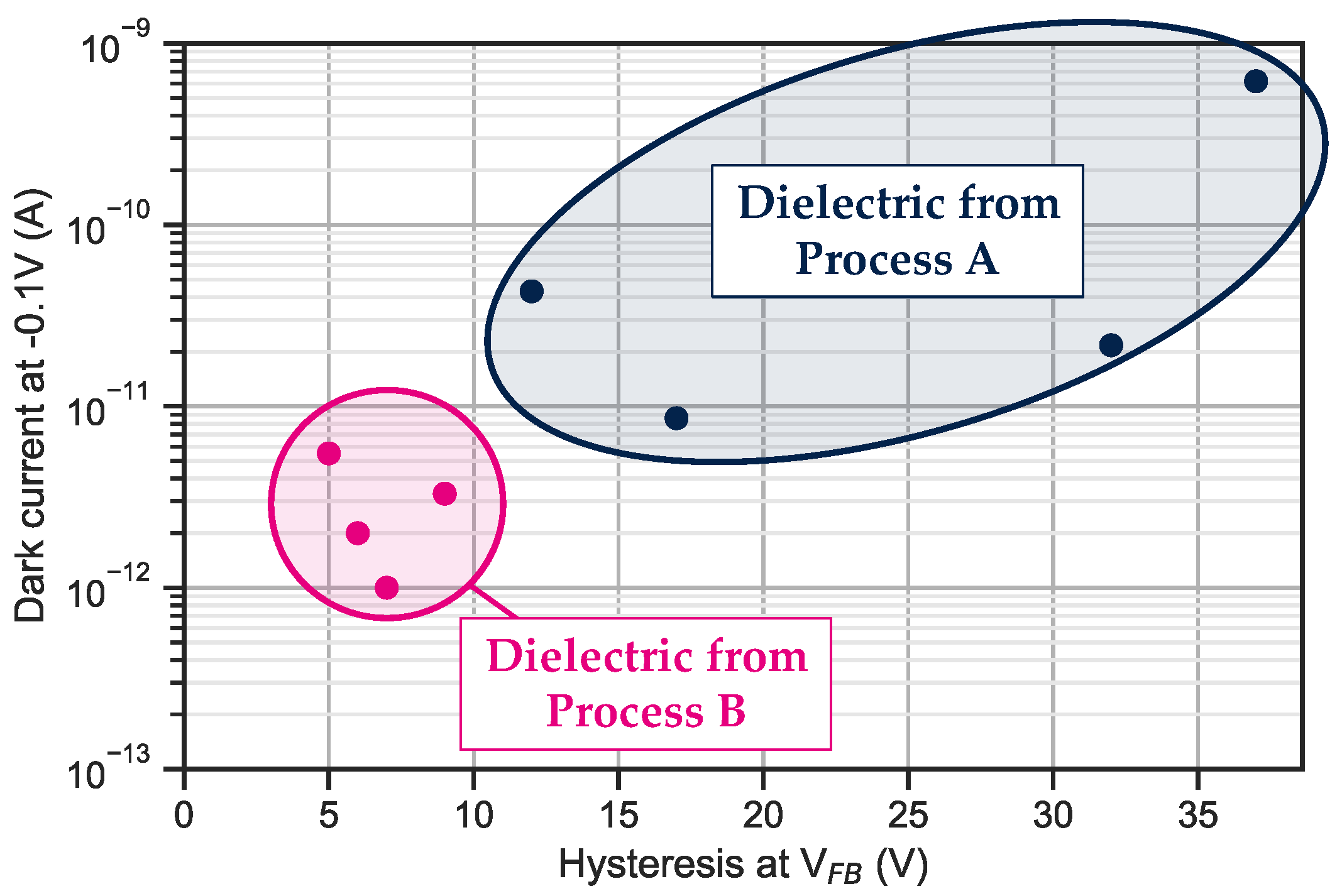
Figure 14. Dark current performances compared to the hysteresis measured on several different wafers.
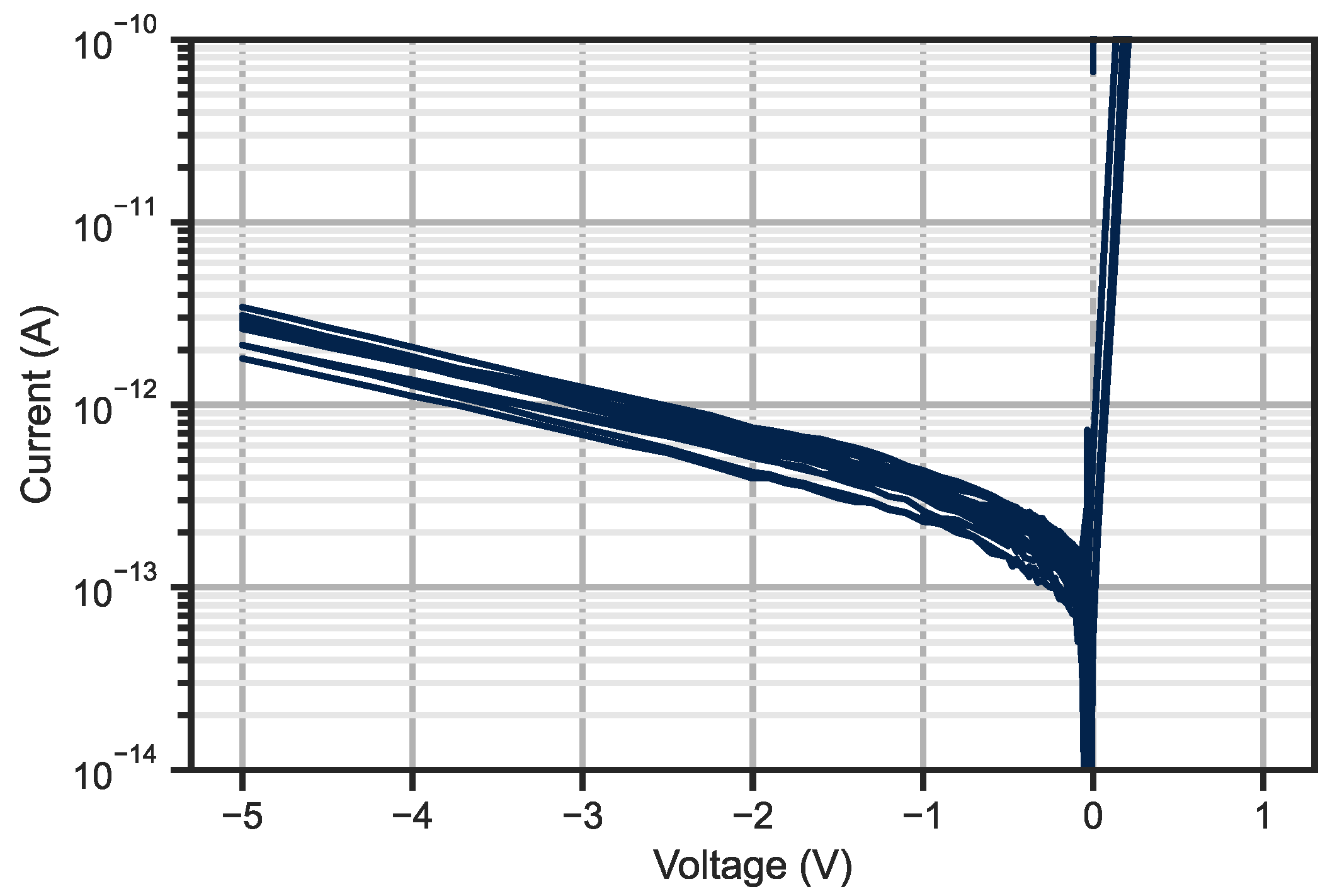
Figure 15. Dark current measurement of a ten-by-ten bundle of 5 μm pixel pitch photodiode. The measurements are conducted at 23 °C.
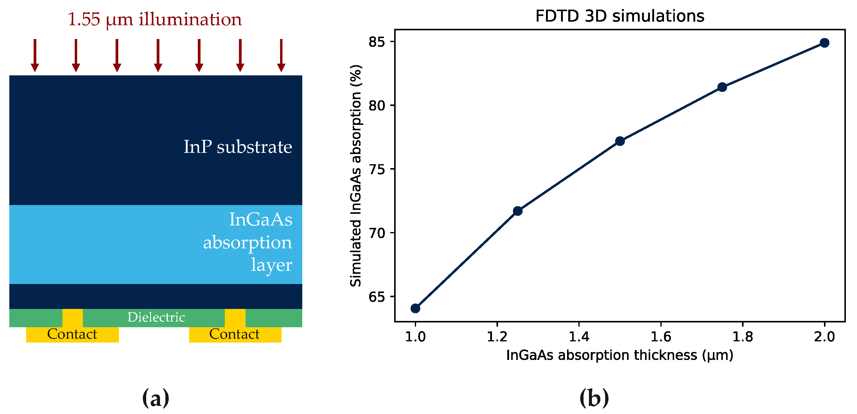
Figure 16. (a) Schematic test structure for QE measurement; (b) the results of the 3D FDTD simulations conducted with Lumerical to estimate the internal QE of the photodiode.

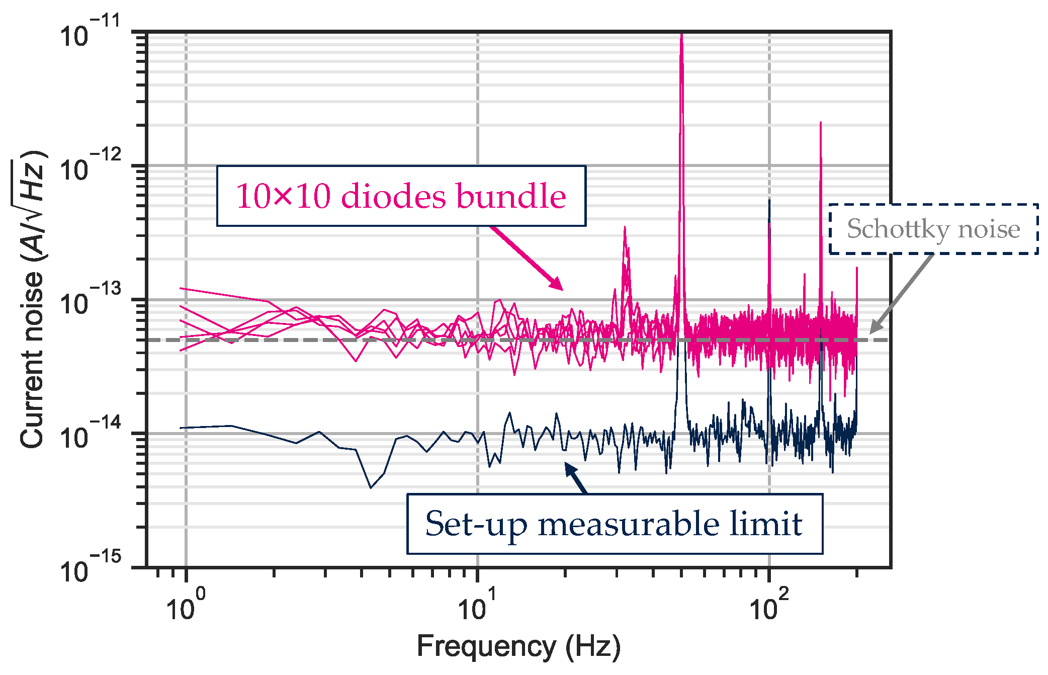
Figure 18. Current noise for a ten-by-ten 5 μm pixel pitch photodiode bundle measured at −0.1 V.
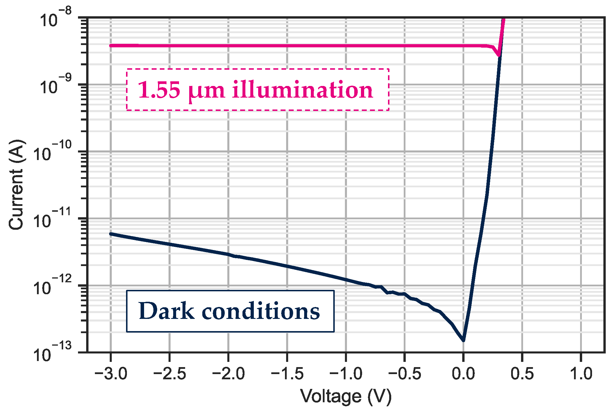
Figure 19. Median current measurement for bundles of one hundred 3 μm pixel pitch photodiodes under dark and SWIR illumination conditions. The dark blue line represents the dark current and the pink line is the photocurrent under 1.55 μm illumination.

Linked to the next post, what is the PD structure that Sony has used in their 3.45um pixel sensor please?
ReplyDelete