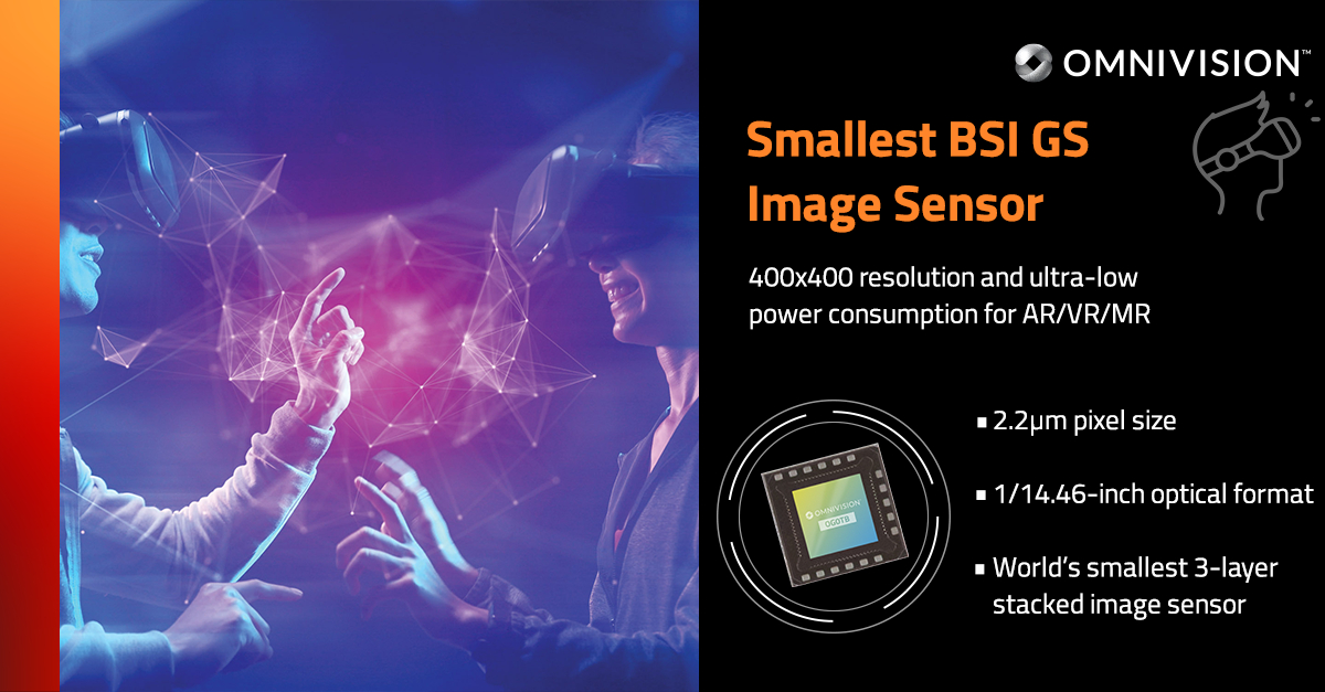
From Businesswire --- "OMNIVISION Announces World’s Smallest Global Shutter Image Sensor for AR/VR/MR and Metaverse".
OmniVision has announced the industry’s first and only three-layer stacked BSI global shutter (GS) image sensor. The OG0TB is the world’s smallest image sensor for eye and face tracking in AR/VR/MR and Metaverse consumer devices, with a package size of just 1.64mm x 1.64mm, it has a 2.2µm pixel in a 1/14.46-inch optical format (OF). The CMOS image sensor features 400×400 resolution and ultra-low power consumption, ideal for some of the smallest and lightest battery-powered wearables, such as eye goggles and glasses. Ultra-low power consumption is critical for these battery-powered devices, which can have 10 or more cameras per system. Their OG0TB BSI GS image sensor consumes less than 7.2mW at 30 frames per second (fps).
SANTA CLARA, Calif.--(BUSINESS WIRE)--OMNIVISION, a leading global developer of semiconductor solutions, including advanced digital imaging, analog, and touch & display technology, today announced the industry’s first and only three-layer stacked BSI global shutter (GS) image sensor. The OG0TB is the world’s smallest image sensor for eye and face tracking in AR/VR/MR and Metaverse consumer devices, with a package size of just 1.64mm x 1.64mm, it has a 2.2µm pixel in a 1/14.46-inch optical format (OF). The CMOS image sensor features 400x400 resolution and ultra-low power consumption, ideal for some of the smallest and lightest battery-powered wearables, such as eye goggles and glasses.
“OMNIVISION is leading the industry by developing the world’s first three-layer stacked global shutter pixel technology and implementing it in the smallest GS image sensor with uncompromising performance,” said David Shin, staff product marketing manager – IoT/Emerging at OMNIVISION. “We pack all of these features and functions into the world’s smallest ‘ready-to-go’ image sensor, which provides design flexibility to put the camera in the most ideal placement on some of the smallest and slimmest wearable devices.” Shin adds, “Ultra-low power consumption is critical for these battery-powered devices, which can have 10 or more cameras per system. Our OG0TB BSI GS image sensor consumes less than 7.2mW at 30 frames per second (fps).”
The worldwide market for AR/VR headsets grew 92.1% year over year in 2021, with shipments reaching 11.2 million units, according to new data from the International Data Corporation (IDC) Worldwide Quarterly AR/VR Headset Tracker1. New entrants as well as broader adoption from the commercial sector will propel the market further as headset shipments are forecast to grow 46.9% year over year in 2022. In fact, IDC expects this market to experience double-digit growth through 2026 as global shipments of AR/VR headsets surpass 50 million units by the end of the forecast, with a 35.1% compounded annual growth rate (CAGR).
OMNIVISION is supporting the growing market for AR/VR headsets by introducing new products such as the OG0TB GS image sensor, which features the company’s most advanced technology:
It is built on OMNIVISION’s PureCel®Plus-S stacked-die technology.
It features a three-layer stacked sensor with pixel size at 2.2µm in a 1/14.46-inch OF to achieve 400x400 resolution.
Nyxel® technology enables the best quantum efficiency (QE) at the 940nm NIR wavelength for sharp, accurate images of moving objects.
The sensor’s high modulation transfer function (MTF) enables sharper images with greater contrast and more detail, which is especially important for enhancing decision-making processes in machine vision applications.
The sensor supports a flexible interface, including MIPI with multi-drop, CPHY, SPI, etc.
The OG0TB GS image sensor will be available for sampling in Q3 2022 and in mass production in the 2H 2023.
PS: It is worth noting that Sony made a claim for "world's first 3 layer stacked CIS" back in 2017 after their ISSCC paper titled "A 1/2.3inch 20Mpixel 3-layer stacked CMOS Image Sensor with DRAM" (DOI: 10.1109/ISSCC.2017.7870268). The three layers consisted of photodiodes, DRAM memory, and mixed-signal ISP. But that was a rolling shutter sensor, whereas this one from OmniVision is a global shutter sensor.
PPS: Readers of blog who know of any journal or conference publication about OmniVision's new design please share them in the comments below!

No comments:
Post a Comment
All comments are moderated to avoid spam and personal attacks.