In a recent paper titled "Design and Characterization of a Burst Mode 20 Mfps Low Noise CMOS Image Sensor" (https://www.mdpi.com/1424-8220/23/14/6356) Xin Yue and Eric Fossum write:
This paper presents a novel ultra-high speed, high conversion-gain, low noise CMOS image sensor (CIS) based on charge-sweep transfer gates implemented in a standard 180 nm CIS process. Through the optimization of the photodiode geometry and the utilization of charge-sweep transfer gates, the proposed pixels achieve a charge transfer time of less than 10 ns without requiring any process modifications. Moreover, the gate structure significantly reduces the floating diffusion capacitance, resulting in an increased conversion gain of 183 µV/e−. This advancement enables the image sensor to achieve the lowest reported noise of 5.1 e− rms. To demonstrate the effectiveness of both optimizations, a proof-of-concept CMOS image sensor is designed, taped-out and characterized.
Have a hard time to understand what the value of this work is. 50+um pixel, very low FWC, huge dark current which makes higher conversion gain useless and the rest of the specifications are also mediocre and weak. It’s like people are out of good ideas and they just want to burn government funds (our tax money).
ReplyDeleteDid you notice the 20 million frames per second frame rate? There are plenty of specialized use cases for extreme frame rates.
DeleteYes, I saw the frame rate. Look at table 6. Do you see way better sensors with higher frame rates, smaller pixels and higher FWC? Yes. So comparing with those sensors, this sensor is mediocre. I would not sign off a PhD thesis that is based on this sensor. Perhaps a Master thesis is ok.
Delete50um pixel with a small full well? Sounds like the specs you would typically want/expect to see in a properly designed 20Mfps sensor. It never makes sense to consider sensor specs. in isolation. There are too many tradeoffs and usually the optimal design is never about achieving the best "numbers" for any particular specification. I would think that clever specmanship for the purpose of impressing the internet is not the goal here.
DeleteSure, let me help.
ReplyDelete1. A 20Mfps sensor has a roughly 50nsec integration time. So one normally wants bigger pixels for better light collection efficiency. 50nsec is about a million times faster than what a normal sensor might integrate for.
2. Likewise, one also does not usually need a big FWC.
3. With low "light" one needs low read noise, so high conversion gain is needed, which limits the FWC.
4. For good charge collection efficiency at such high speeds with large pixels, one needs pretty strong electric fields, so dark current is typically high in such a high speed image sensor compared to the same process but with lower electric fields.
5. It is a nice piece of technical work, start to finish, by Xin Yue, a well regarded experienced design engineer in the field of high speed sensors, who came back to graduate school (Dartmouth) to learn more about image sensor device physics and pixels. I just wish we had had access to a 3D BSI stacked process. Instead, Xin did the best design he could in a standard (unmodified) 180nm process. Quite good performance for an unmodified process. Perhaps the world record for speed for a modified process device is held by Prof. Kuroda's group at Tohoku University. Prof. Kuroda also served on Xin's PhD committee (thank you again Rihito).
6. We were asked by the US Govt. to explore this sort of sensor to pave the way for larger more sophisticated sensors.
7. Some of this work was already presented at Electronic Imaging (design part) and at IISW (some of the results). It seemed to be well received as a flash presentation of this work was done during the Covid pandemic. It was extra hard to get access to chip fabrication much less any sort of process modification.
I hope this is helpful.
1. Based on paper, you ran the sensor at 4mfps, not 20mfps. Measurements vs simulation (reality vs dream). Let’s say 20mfps, based on table 6 in paper, there are sensors, with larger arrays and smaller pixel sizes can go more than 300mfps. So no improvements here.
Delete2. FWC is important. And again table 6 shows sensors with better specs with way higher FWC. So no improvement here.
3. CG is relatively better than the sensors listed in table 6, however, there have been way higher CG sensors reported before. So no improvement here. Should mention very low FF.
4. Your DC is high also because the pixel is so large. Again, there are way smaller pixels with better specifications listed in table 6. So no improvement here either.
5. Table 6 shows other works with old technologies who could achieve better results. So no improvement here either.
6. Maybe instead of jumping on this design so fast, more feasibility study could be done. With access to great CAD tools these days, it’s a no brainer.
7. Based on the results presented and table 6, this work does not provide any notable improvements to the state of the art.
Good luck for your next research work.
If you look at all these specs in isolation, then yes. But that's not how to evaluate imagers.
DeleteJust shaking my head. Thanks anonymous troll. We all missed you.
DeleteIn my opinion, anonymous has a point. Why shake your head? And why call the person troll? The reasoning makes sense based on table 6 (comparison table) in the paper. There are sensors have better specs. I see sensors with smaller pixels in a larger array, with higher frame rate and FWC, made with kind of similar older process. Am I missing something here?
DeleteThis comment has been removed by a blog administrator.
DeleteI don’t see any trolling. Valid points.
DeleteNice conversation with yourself, anonymous.
DeleteMeanwhile let's talk about MDPI Sensors journal since you just insulted anyone who publishes in that journal. Your statement is probably legally libelous: "as long as you pay the expensive fees, they publish your paper," but that is between MDPI and you.
-IEEE also charges high fees for open access with a lot less service and often much slower turn-around time. The IEEE journals are great, and charging a fee is not indicative of low quality.
-Reviewers for all journals can vary. But for example, for IISW special issues, we have partnered with MDPI Sensors, and the reviewers for those papers are typically from well-respected members of image sensor technical community and the academic editorial review process is governed by IISS.
-For sure MDPI Sensors actively solicits (good) papers, and has way too many special issues on image sensors. But, generally publishing papers on image sensors is good for the image sensor community, whether it be IEEE or MDPI or Optica or SPIE.
-As you mention, IEEE JSSC has very high standards and tends to cater toward commercial work rather than exploratory research work. You had best have stellar, highly competitive performance to report or the paper may not be selected, and it had best be oriented towards circuits, not optics nor devices.
-Xin's paper was not shopped around and we decided to put it in MDPI Sensors as an appropriate journal. Other papers from IISW will be published in a forthcoming special issue in MDPI Sensors, as I understand it. One of the reasons we selected Sensors was because of their high efficiency in moving papers along. They are very fast at getting papers through the publishing production process. IEEE is much slower.
-The 3 reviewers for our paper did a good job of illuminating improvement areas, but were also very positive about the work. Their comments definitely made the paper stronger.
-Impact Factor is not a metric I am fond of, but here are recent impact factors as returned by a google search. I don't think an 2x difference in impact factor is all that significant, given other factors, but here they are:
IEEE JSSC 5.4
IEEE EDL 4.8
MDPI Sensors 3.8
IEEE TED 3.1
IEEE JEDS 2.53
This comment has been removed by a blog administrator.
DeleteI don't know who is behind the predatory reports website, but they remain anonymous and acknowledge it is a group of academics that believe they have been harmed by predatory publishers. They have a very very long black list but no explanation of why journals are there or not there. There is some discussion about MDPI but it quotes something from 2014 which was actually reversed in 2015 after an investigation. That seems odd to not mention that reversal. Wikipedia, also known for total veracity (not!) does speak more even-handedly of negatives and positives and it is good to read it, eyes wide open and all. MDPI seems to have been investigated several times but typically comes up exonerated. It seems funny that you claim Wikipedia is "reality" and certainly the other website seems highly biased. And who likes long black lists without accompanying evidence?
DeleteBut, all I really know for sure, i.e. my reality, is my own experience and that of IISW's special issues. I believe those experiences have all been positive. You can check with those involved at IISS, you don't have to take my word for it. BTW, there was some nervousness with the first IISW special issue due to some of these early predatory "reports" and exonerations, but we have not had a problem thus far.
From a peer review point of view, I would say the reviewer quality is about as mixed for IEEE TED/JEDS/JSSC as it is for MDPI Sensors. The costs have been sort of similar, but in the case of MDPI, I feel one gets actual editorial and publication processing value for the expense, not so much with IEEE.
In the case of MDPI Sensors, it seems wrong to label them as less professional compared to IEEE. Of course MDPI has a lot of journals and some editors may be more professional than others. IEEE and MDPI are both net-revenue-focused operations, whether or not they are non-profit or for-profit.
I publish in IEEE TED and JEDS, and also MDPI Sensors. Personally I think TED and JEDS are redundant once TED introduced open-access policies and fees, These days, with Google Scholar searches, you can easily find articles of interest independent of where they are published.
Eric, there is a saying: “if you’re explaining, you’re losing.” I see you’re constantly doing it. There is a published work, and the paper is more than 15 pages long. All these had to be explained in the paper and if this much explaining is needed now, after it’s published, maybe it wasn’t ready for publishing. Just my 2 cents.
DeleteN.D.
@N.D. I don't imagine this saying applies to professors. It is our job to explain and help people understand things. You are right, all this stuff was in the paper. But, probably most people don't actually read the paper in detail, and for many, hearing an explanation in different words can be helpful.
Delete20Mfps realized by 0.18um CIS process is impressive. However, dark current ~ 0.46e-/ns/pixel, which means it's like a 10uW/cm^2 green light illuminating on the pixel. (Here I assume total QE~60%, pixel area~2788um^2, and all area could collect photons.) In other words, if the light source is weaker than 683Lux (100uW/cm^2), the pixel will suffer from dark current even just at 300K. I'm not sure if this design matches the environment conditions in most of high speed applications.
ReplyDeleteThe dark current is high and probably needs further investigation prior to committing to a full size sensor. The most likely cause is related to high electric fields and with some process modification that can likely be ameliorated. For the anticipated application the dark current is ok, and the camera/sensor can be cooled if need be. The anticipated application "lighting" is not like most other high-speed applications, or even other ultra-high-speed applications.
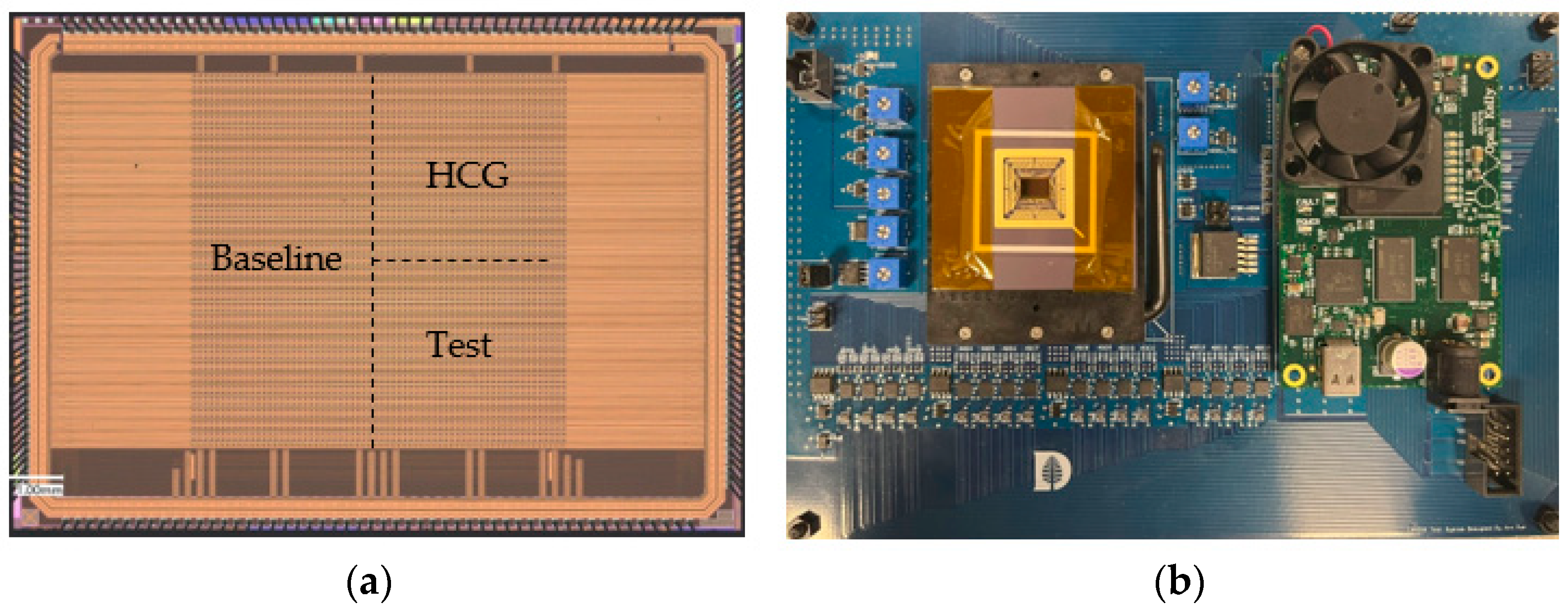
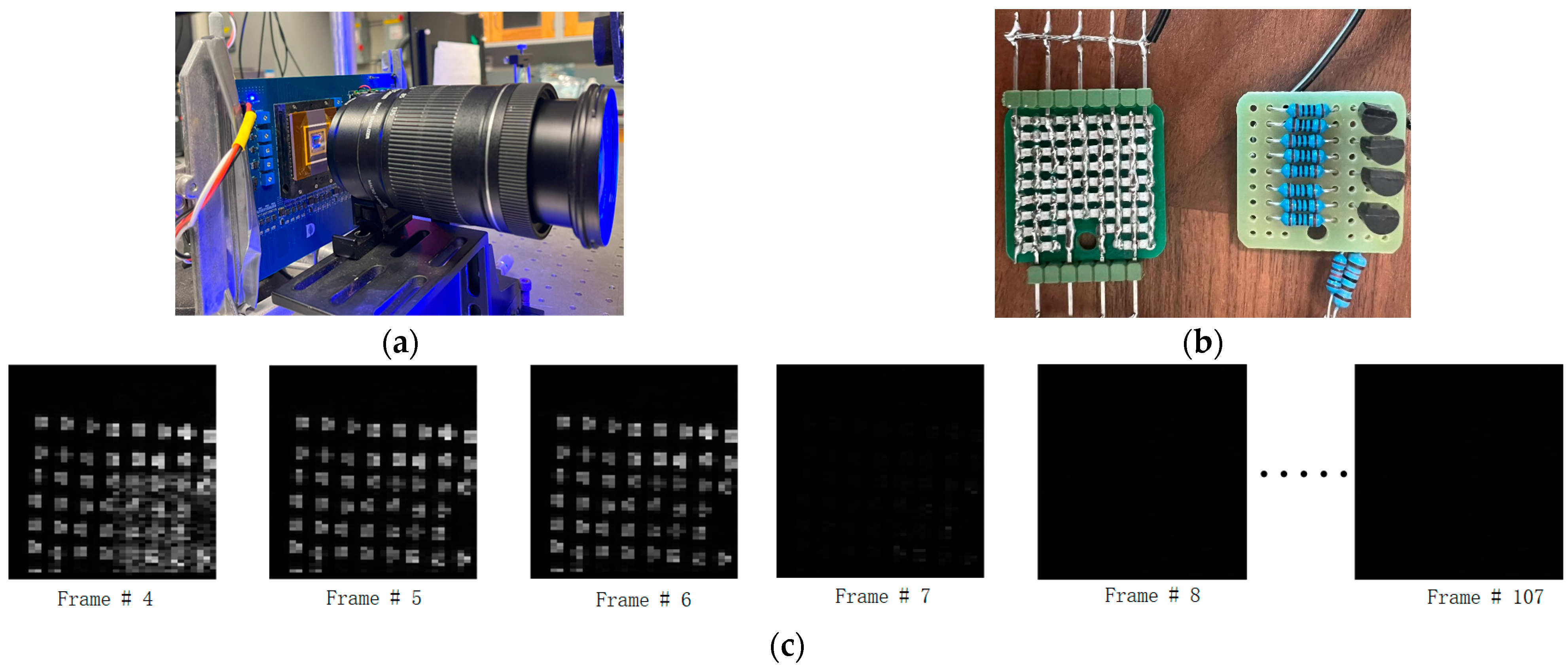
ReplyDeleteLooking at figure 15 a, I hope it’s not the setup was used to test and measure sensor. I can see major flaws with this set up.
ReplyDeleteIt is so easy to add negative comments under the heading of "Anonymous", irrespective whether the content of your comments makes sense or not. You would show a great responsability and courage if you could disclose who you are, independent whether your comments are positive or negative. That would make the quality and the impact of your comments much higher. But after all you are a free person ....
ReplyDeleteHi Albert. Indeed. Anonymous replies on this forum have mostly been trolls the last years. Rarely anything meaningful is posted anonymously. Maybe, while this forum is being refreshed, finally, it’s time to turn off anonymous replies?
DeleteJonathan Borremans
Sometimes people backlash if posting with real name and address, especially if you are just starting out, and are considered "weak" or too "strong". Anonymity in principle allows more freedom to put out opinions. If you are well informed to separate the chaff from the grain, be free to post counter opinions
DeleteThe "Anonymous" signature makes it possible to post information that might get the submitter in trouble with an employer. I wouldn't delete Anonymous but I would improve the moderation. Aside from the obvious troll posts, the one above about the test setup is useless without an explanation of what the submitter finds wrong.
DeleteIn my honest opinion, it should not matter who the commenter is. We should pay attention to the message. What I see here is some posters who they comment with they real names, their comments are written with some sense of bullying to just undermine the commenter, instead of responding to the critical comments or questions asked.
DeleteEven if you got rid of the option to post anonymously, what would stop someone from coming up with a fake name?
Deletei post anonymous because my company does not want to publish what we are working on. ok - a fake name/account would be a way out ;-) not all people are fans of the current social media 'everyone on earth has to know every little thing i do' wave. apart from trying not to disclose things, I dislike to publish publically, i also do not post my bike tour stats or what i eat for dinner ;-)
DeleteI suggest Vladimir deletes and not approve useless comments. I would delete all the comments above about the journals.
ReplyDeleteNot at all, some ( large) amount of freedom of speech should be tolerated.
DeleteThis comment has been removed by a blog administrator.
ReplyDeleteMy two cents. I don't understand why anonymous saids that small pixels are better than big pixels. For sure that using small pixels is much easy to achieve a high resolution sensor. And also is easier to do the pixels faster. However, small pixels are useless if the amount of light is very small or if the speed is very high. The problem is that in a small pixel with low light and/or very short exposure time, the amount of integrated charge is almost zero. Then, hasn't sense at all to have a high FWC if you cannot integrate more than few electrons (or holes) per frame. The main advantage of this work is that obtain ultra high speed sensor at the same time that they use big pixels. The use of big pixels isn't a problem, but an advantage.
ReplyDeleteNot when your fill factor is less than 10%. Basically, 90% of the big pixel does not gather light. You use the “2 cents” phrase when you have a point, not for asking question or a doubtful statement.
DeleteHere is my 2 cents. Big pixels help with light gathering, and in this work, the pixel area is used for 108 frames of analog memory as well, since it is a non-stacked FSI process. Obviously, as stated in the paper, if a 3D stacked BSI process was available, the memory would be a on different stack level and the effective fill factor could be larger. For "hyper-active" pixels, fill factor is always an issue, starting from global shutter, to DVS, SPADS and high energy physics detectors.
DeleteAnonymous. Who are you to say me how must I use the language? In my opinion I have apported or reinforced significant information. If you prefer to discuss more directly, you can publicate your identity or contact and we can discuss privately. In other case, you must accept the critics from other readers. Even if we may be wrong.
Delete