UnwiredView.com noticed that USPTO published Nokia patent application US20120205518:
"Sensing of Photons" by Martti Voutilainen, Markku Rouvala, and Pirjo Pasanen.
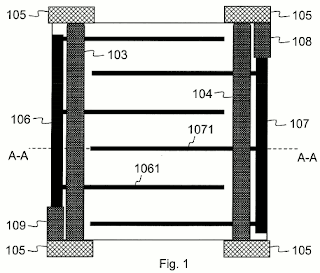
The sensor consists of multiple light-sensitive layers of graphene connected to the gates of graphene amplifying FET 106 and 107 and to source of graphene reset transistor 108. Fig. 1 shows a horizontal structure of the pixel, while Fig. 2 shows the vertical cross-section together with RGB color filters 221-223:


Well, the literature is definitely sparse on graphene photodetection. Guess it is the missing bandgap or the short carrier lifetime. I wonder how Nokia will argue enablement down the road?
ReplyDeleteThere are a number of papers claiming generation of a bandgap in graphene. Here's a couple:
ReplyDelete"Observation of an electrically tunable band gap in trilayer graphene": http://www.nature.com/nphys/journal/v7/n12/full/nphys2102.html
"Tunable and sizable band gap of single-layer graphene sandwiched between hexagonal boron nitride": http://www.nature.com/am/journal/v4/n2/full/am201210a.html
Yes I have seen these and others, but graphene itself does not have a bandgap. I don't think these devices above are too good for image sensors, but more importantly, they are not in the patent application. In my opinion their teaching does not enable one to make the device described, nor is it apparent to one skilled in the art (me, for example) how to make an image sensor using graphene based on the teaching of the application.
ReplyDeleteI will say that it is important that we, as a community, think about how we will build image sensors when the silicon structures we use today are not easily available in future mainstream processes. I think we may have to separate detection and integration (and readout), but perhaps stacked structures will allow us to mix and match materials, not unlike IR FPAs.
I think the idea that patents should allow someone skilled in the art to build the thing, was thrown out long ago!
DeleteYes, I agree that stacked heterogenous structures will be the future for image sensors. In a way it is a return to the past (a past that of course still persists for LWIR), but it will be analogous to modern commercial BSI versus old-fashioned, hand-polished BSI.
"No BAND GAP!" you say.
ReplyDeleteBuild A New Device (claim one)
Graphene APS?
(some haiku acronym fun)
DeleteEven were enablement satisfied, it seems to me that the claims just recite structures analogous to existing CMOS APS approaches. It's difficult for me to see how any of them are not obvious if you happen to have graphene photodetectors and transistors.
Delete