Monday, June 30, 2025

MIPI C-PHY v3.0 upgrades data rates

News: https://www.businesswire.com/news/home/20250507526963/en/MIPI-C-PHY-v3.0-Adds-New-Encoding-Option-to-Support-Next-Generation-of-Image-Sensor-Applications

The MIPI Alliance, an international organization that develops interface specifications for mobile and mobile-influenced industries, today announced a major update to its high-performance, low-power and low electromagnetic interference (EMI) C-PHY interface specification for connecting cameras and displays. Version 3.0 introduces support for an 18-Wirestate mode encoding option, increasing the maximum performance of a C-PHY lane by approximately 30 to 35 percent. This enhancement delivers up to 75 Gbps over a short channel, supporting the rapidly growing demands of ultra-high-resolution, high-fidelity image sensors.

The new, more efficient encoding option, 32b9s, transports 32 bits over nine symbols and maintains MIPI C-PHY’s industry-leading low EMI and low power properties. For camera applications, the new mode enables the use of lower symbol rates or lane counts for existing use cases, or higher throughput with current lane counts to support new use cases involving very high-end image sensors such as:

  •  Next-generation prosumer video content creation on smartphones, with high dynamic range (HDR), smart region-of-interest detection and advanced motion vector generation
  •  Machine vision quality-control systems that can detect the smallest of defects in fast-moving production lines
  •  Advanced driver assistance systems (ADAS) in automotive that can analyze the trajectory and behavior of fast-moving objects in the most challenging lighting conditions 
C-PHY Capabilities and Performance Highlights
MIPI C-PHY supports the MIPI Camera Serial Interface 2 (MIPI CSI-2) and MIPI Display Serial Interface 2 (MIPI DSI-2) ecosystems in low-power, high-speed applications for the typical interconnect lengths found in mobile, PC compute and IoT applications. The specification:
  •  Provides high throughput, a minimized number of interconnect signals and superior power efficiency to connect cameras and displays to an application processor. This is due to efficient three-phase coding unique to C-PHY that reduces the number of system interconnects and minimizes electromagnetic emissions to sensitive RF receiver circuitry that is often co-located with C-PHY interfaces.
  •  Offers flexibility to reallocate lanes within a link because C-PHY functions as an embedded clock link
  •  Enables low-latency transitions between high-speed and low-power modes
  •  Includes an alternate low power (ALP) feature, which enables a link operation using only C-PHY’s high-speed signaling levels. An optional fast lane turnaround capability utilizes ALP and supports asymmetrical data rates, which enables implementers to optimize the transfer rates to system needs.
  •  Can coexist on the same device pins as MIPI D-PHY, so designers can develop dual-mode devices
Support for C-PHY v3.0 was included in the most recent MIPI CSI-2 v4.1 embedded camera and imaging interface specification, published in April 2024. To aid implementation, C-PHY v3.0 is backward-compatible with previous C-PHY versions.

“C-PHY is MIPI's ternary-based PHY for smartphones, IoT, drones, wearables, PCs, and automotive cameras and displays,” said Hezi Saar, chair of MIPI Alliance. “It supports low-cost, low-resolution image sensors with fewer wires and high-performance image sensors in excess of 100 megapixels. The updated specification enables forward-looking applications like cinematographic-grade video on smartphones, machine vision quality-control systems and ADAS applications in automotive.”

Forthcoming MIPI D-PHY Updates
Significant development work is continuing on MIPI's other primary shorter-reach physical layer, MIPI D-PHY. D-PHY v3.5, released in 2023, includes an embedded clock option for display applications, while the forthcoming v3.6 specification will expand embedded clock support for camera applications, targeting PC / client computing platforms. The next full version, v4.0, will further expand D-PHY’s embedded clock support for use in mobile and beyond-mobile machine vision applications, and further increase D-PHY’s data rate beyond its current 9 Gbps per lane.

Also, MIPI Alliance last year conducted a comprehensive channel signal analysis to document the longer channel lengths of both C- and D-PHY. The resulting member application note, "Application Note for MIPI C-PHY and MIPI D-PHY IT/Compute," demonstrated that both C-PHY and D-PHY can be used in larger end products, such as laptops and all-in-ones, with minimal or no changes to the specifications as originally deployed in mobile phones or tablets, or for even longer lengths by operating at a reduced bandwidth. 
Sunday, June 29, 2025

NIT announces SWIR line sensor

New SWIR InGaAs Line Scan Sensor NSC2301 for High-Speed Industrial Inspection

New Imaging Technologies (NIT) announces the release of its latest SWIR InGaAs line scan sensor,
the NSC2301, designed for demanding industrial inspection applications. With advanced features and
performance, this new sensor sets a benchmark in SWIR imaging for production environments.

Key features

  • 0.9µm to 1.7µm spectrum
  • 2048x1px @8µm pixel pitch
  • 90e- readout noise
  • Line rate >80kHz @ 2048 pixel resolution
  • Single stage TEC cooling
  • Configurable exposure times
  • ITR & IWR readout modes

The NSC2301 features a 2048 x 1 resolution with an 8 µm pixel pitch, delivering sharp, detailed line-
scan imaging. The size format is best suited to fit standard 1.1’’ optical format optics. This SWIR line-
scan sensor supports line rates over 80 kHz, making it ideal for fast-moving inspection tasks.
With configurable exposure times and both ITR (Integration Then Read) and IWR (Integration While
Read) readout modes, the sensor offers unmatched adaptability for various lighting and motion
conditions.

Thanks to its 3 gains available, the NSC2301 provides the perfect combination of High Sensitivity
(read out noise 90e- in High Gain) and High Dynamic Range, crucial for imaging challenging materials
or capturing subtle defects in high-speed production lines.

This new sensor expands NIT’s proprietary SWIR sensor portfolio and will be officially introduced
at Laser World of Photonics 2025 in Munich.

Applications
Typical use cases for the NSC2301 include silicon wafer inspection, solar panel inspection, hot glass
quality control, waste sorting, and optical coherence tomography, especially where high-resolution
and high-speed line-scan imaging is critical.

Camera
Complementing the launch of the sensor, NIT will release LiSaSWIR v2, a high-performance camera
integrating the NSC2301, in late summer. The camera will feature Smart CameraLink for fast data
transmission and plug-and-play integration.
With the NSC2301, NIT continues its mission of delivering cutting-edge SWIR imaging technology,
developed and produced in-house.

Friday, June 27, 2025

TechInsights blog on Samsung's hybrid bond image sensor

Link: https://www.techinsights.com/blog/samsung-unveils-first-imager-featuring-hybrid-bond-technology

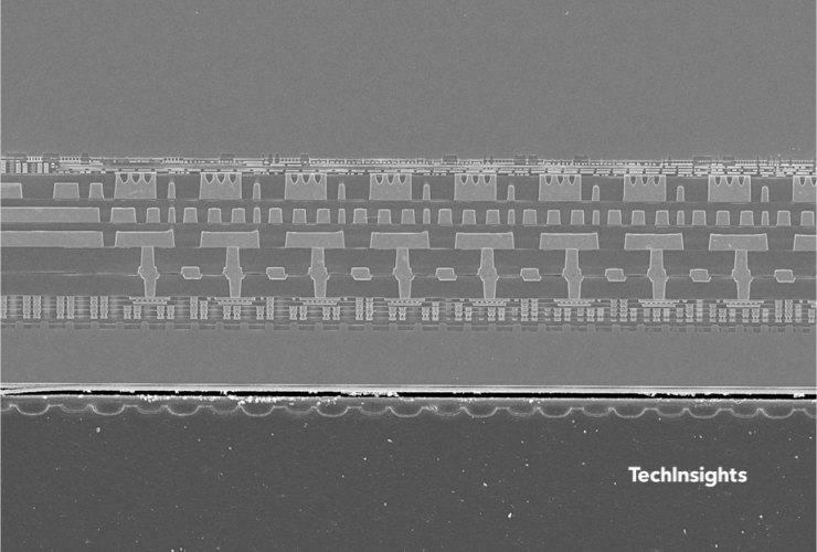
In a recent breakthrough discovery by TechInsights, the Samsung GM5 imager, initially thought to be a standard back-illuminated CIS, has been revealed to feature a pioneering hybrid bond design. This revelation comes after a year-long investigation following its integration into the Google Pixel 7 Pro.

Initially cataloged as a regular back-illuminated CIS due to the absence of through silicon vias (TSVs), further analysis was prompted by its appearance in the Google Pixel 8 Pro, boasting remarkable resolution. This led to an exploratory cross-section revealing the presence of a hybrid bond, also known as Direct Bond Interconnect (DBI). 


Wednesday, June 25, 2025

Webinar on image sensors for astronomy


The Future of Detectors in Astronomy


In this webinar, experts from ESO and Caeleste explore the current trends and future directions of detector technologies in astronomy. From ground-based observatories to cutting-edge instrumentation, our speakers share insights into how sensor innovations are shaping the way we observe the universe.
 

Speakers:
Derek Ives (ESO) – Head of Detector Systems at ESO
Elizabeth George (ESO) – Detector Physicist
Ajit Kalgi (Caeleste) – Director of Design Center
Jan Vermeiren (Caeleste) – Business Development Manager

Monday, June 23, 2025

Open Letter from Johannes Solhusvik, New President of the International Image Sensor Society (IISS)

Dear all, 
 
As announced by Junichi Nakamura during the IISW’25 banquet dinner, I have now taken over as President of the International Image Sensor Society (IISS). I will do my best to serve the imaging community and to ensure the continued success of our flagship event the International Image Sensor Workshop (IISW). 
 
The workshop objective is to provide an opportunity to exchange the latest progress in image sensor and related R&D activities amongst the top image sensor technologists in the world in an informal atmosphere. 
 
With the retirement of Junichi Nakamura from the Board, as well as Vladimir Koifman who also completed his service period, two very strong image sensor technologists have joined the IISS Board, namely Min-Woong Seo (Samsung) and Edoardo Charbon (EPFL). Please join me in congratulating them. 
 
Finally, I would like to solicit any suggestions and insights from the imaging community how to improve the IISS and to start planning your paper submission to the next workshop in Canada in 2027. More information will be provided soon at our website www.imagesensors.org 
 
Best regards, 
 
Johannes Solhusvik 
President of IISS 
VP, Head of Sony Semiconductor Solutions Europe

Friday, June 20, 2025

Sony IMX479 520-pixel SPAD LiDAR sensor

Press release: https://www.sony-semicon.com/en/news/2025/2025061001.html

Sony Semiconductor Solutions to Release Stacked SPAD Depth Sensor for Automotive LiDAR Applications, Delivering High-Resolution, High-Speed Performance High-resolution, high-speed distance measuring performance contributes to safer, more reliable future mobility

Atsugi, Japan — Sony Semiconductor Solutions Corporation (SSS) today announced the upcoming release of the IMX479 stacked, direct Time of Flight (dToF) SPAD depth sensor for automotive LiDAR systems, delivering both high-resolution and high-speed performance.

The new sensor product employs a dToF pixel unit composed of 3×3 (horizontal × vertical) SPAD pixels as a minimum element to enhance measurement accuracy using a line scan methodology. In addition, SSSs proprietary device structure enables a frame rate of up to 20 fps, which is the fastest for such a high-resolution SPAD depth sensor having 520 dToF pixels. 

The new product enables the high-resolution and high-speed distance measuring performance demanded for an automotive LiDAR required in advanced driver assistance systems (ADAS) and automated driving (AD), contributing to safer and more reliable future mobility. 

LiDAR technology is crucial for the high-precision detection and recognition of road conditions and the position and shape of the objects, such as vehicles, pedestrians. There is a growing demand for further technical advancements and developments progress in LiDAR toward Level 3 automated driving, which allows for autonomous control. SPAD depth sensors use the dToF measurement method, one of the LiDAR ranging methods, that measures the distance to an object by detecting the time of flight (time difference) of light emitted from a source until it returns to the sensor after being reflected by the object.

The new sensor harnesses SSS’s proprietary technologies acquired in the development of CMOS image sensors, including the back-side illuminated, stacked structure and Cu-Cu (copper-copper) connections. By integrating the newly developed distance measurement circuits and dToF pixels on a single chip, the new product has achieved a high-speed frame rate of up to 20 fps while delivering a high resolution of 520 dToF pixels with a small pixel size of 10 μm square.

Main Features
■ Up to 20 fps frame rate, the fastest for a 520 dToF pixel SPAD depth sensor

This product consists of a pixel chip (top) with back-illuminated dToF pixels and a logic chip equipped with newly developed distance measurement circuits (bottom) using a Cu-Cu connection on a single chip. This design enables a small pixel size of 10 μm square, achieving high resolution of 520 dToF pixels. The new distance measurement circuits handle multiple processes in parallel for even better high-speed processing.

These technologies achieve a frame rate of up to 20 fps, the fastest for a 520 dToF pixel SPAD depth sensor. They also deliver capabilities equivalent to 0.05 degrees vertical angular resolution, improving the vertical detection accuracy by 2.7 times that of conventional products. These elements allow detection of three-dimensional objects that are vital to automotive LiDAR, including objects as high as 25 cm (such as a tire or other objects in the road) at a distance of 250 m.

■ Excellent distance resolution of 5 cm intervals
The proprietary circuits SSS developed to enhance the distance resolution of this product individually processes each SPAD pixel data and calculates the distance. Doing so successfully improved the LiDAR distance resolution to 5 cm intervals.

■ High, 37% photon detection efficiency enabling detection of objects up to a distance of 300 m
This product features an uneven texture on both the incident plane and the bottom of the pixels, along with an optimized on-chip lens shape. Incident light is diffracted to enhance the absorption rate to achieve a high, 37% photon detection efficiency for the 940 nm wavelength, which is commonly used on automotive LiDAR laser light sources. It allows the system to detect and recognize objects with high precision up to 300 m away even in bright light conditions where the background light is at 100,000 lux or higher.


Wednesday, June 18, 2025

Artilux and VisEra metalens collaboration

News release: https://www.artiluxtech.com/resources/news/1023

Artilux, the leader of GeSi (germanium-silicon) photonics technology and pioneer of CMOS (complementary metal-oxide-semiconductor) based SWIR (short-wavelength infrared) optical sensing, imaging and communication, today announced its collaboration with VisEra Technologies (TWSE: 6789) on the latest Metalens technology. The newly unveiled Metalens technology differs from traditional curved lens designs by directly fabricating, on a 12” silicon substrate, fully-planar and high-precision nanostructures for precise control of light waves. By synergizing Artilux’s core GeSi technology with VisEra’s advanced processing capabilities, the demonstrated mass-production-ready Metalens technology significantly enhances optical system performance, production efficiency and yield. This cutting-edge technology is versatile and can be broadly applied in areas such as optical sensing, optical imaging, optical communication, and AI-driven commercial applications.

Scaling the Future: Opportunities and Breakthroughs in Metalens Technology
With the rise of artificial intelligence, robotics, and silicon photonics applications, silicon chips implemented for optical sensing, imaging, and communication are set to play a pivotal role in advancing these industries. As an example, smartphones and wearables having built-in image sensing, physiological signal monitoring, and AI-assistant capabilities will become increasingly prevalent. Moreover, with high bandwidth, long reach, and power efficiency advantages, silicon photonics is poised to become a critical component for supporting future AI model training and inference in AI data centers. As hardware designs require greater miniaturization at the chip-level, silicon-based "Metalens” technology will lead and accelerate the deployment of these applications.

Metalens technology offers the benefits of single-wafer process integration and compact optical module design, paving the way for silicon chips to gain growth momentum in the optical field. According to the Global Valuates Reports, the global market for Metalens was valued at US$ 41.8 million in the year 2024 and is projected to reach a revised size of US$ 2.4 billion by 2031, growing at a CAGR up to 80% during the forecast period 2025-2031.

Currently, most optical systems rely on traditional optical lenses, which utilize parabolic or spherical surface structures to focus light and control its amplitude, phase, and polarization properties. However, this approach is constrained by physical limitations, and requires precise mechanical alignment. Additionally, the curved designs of complex optical components demand highly accurate coating and lens-formation processes. These challenges make it difficult to achieve wafer-level integration with CMOS-based semiconductor processes and optical sensors, posing a significant hurdle to the miniaturization and integration of optical systems.

Innovative GeSi and SWIR Sensing Technology Set to Drive Application Deployment via Ultra-Thin Optical Modules
Meta-Surface technology is redefining optical innovation by replacing traditional curved microlenses with ultra-thin, fully planar optical components. This advancement significantly reduces chip size and thickness, increases design freedom for optical modules, minimizes signal interference, and enables precise optical wavefront control. Unlike the emitter-end DOE (Diffraction Optical Element) technology, Artilux’s innovative Metalens technology directly manufactures silicon-based nanostructures on 12” silicon substrates with ultra-high precision. By seamlessly integrating CMOS processes and core GeSi technology on a silicon wafer, this pioneering work enhances production efficiency and yield rates, supporting SWIR wavelengths. With increased optical coupling efficiency, this technology offers versatile solutions for AI applications in optical sensing, imaging, and communication, catering to a wide range of industries such as wearables, biomedical, LiDAR, mixed reality, aerospace, and defense.

Neil Na, Co-Founder and Chief Technology Officer of Artilux, stated, "Artilux has gained international recognitions for its innovations in semiconductor technology. We are delighted to once again share our independently designed Meta-Surface solution, integrating VisEra's leading expertise in 12” wafer-level optical manufacturing processes. This collaboration successfully creates ultra-thin optical components that can precisely control light waves, and enables applications across SWIR wavelength for optical sensing, optical imaging, optical communication and artificial intelligence. We believe this technology not only holds groundbreaking value in the optical field but will also accelerate the development and realization of next-generation optical technologies."

JC Hsieh, Vice President in Research and Development Organization of VisEra, emphasized, "At VisEra, we continuously engage in global CMOS imaging and optical sensor industry developments while utilizing our semiconductor manufacturing strengths and key technologies R&D and partnerships to enhance productivity and efficiency. We are pleased that our business partner, Artilux, has incorporated VisEra’s silicon-based Metalens process technology to advance micro-optical elements integration. This collaboration allows us to break through conventional form factor limitations in design and manufacturing. We look forward to our collaboration driving more innovative applications in the optical sensing industry and accelerating the adoption of Metalens technology."

Metalens technology demonstrates critical potential in industries related to silicon photonics, particularly in enabling miniaturization, improved integration, and enhanced performance of optical components. As advancements in materials and manufacturing processes continue to refine the technology, many existing challenges are gradually being overcome. Looking ahead, Metalens are expected to become standard optical components in silicon photonics and sensing applications, driving the next wave of innovation in optical chips and expanding market opportunities.


Monday, June 16, 2025

Zaber application note on image sensors for microscopy

Full article link: https://www.zaber.com/articles/machine-vision-cameras-in-automated-microscopy

When to Use Machine Vision Cameras in Microscope
Situation #1: High Throughput Microscopy Applications with Automated Image Analysis Software
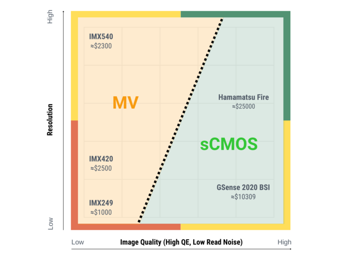
Machine vision cameras are ideally suited to applications which require high throughput, are not limited by low light, and where a human will not look at the raw data. Designers of systems where the acquisition and analysis of images will be automated must change their perspective of what makes a “good” image. Rather than optimizing for images that look good to humans, the goal should be to capture the “worst” quality images which can still yield unambiguous results as quickly as possible when analyzed by software. If you are using “AI”, a machine vision camera is worth considering.
A common example is imaging consumables to which fluorescent markers will hybridize to specific sites. To read these consumables, one must check each possible hybridization site for the presence or absence of a fluorescent signal.

Situation #2: When a Small Footprint is Important
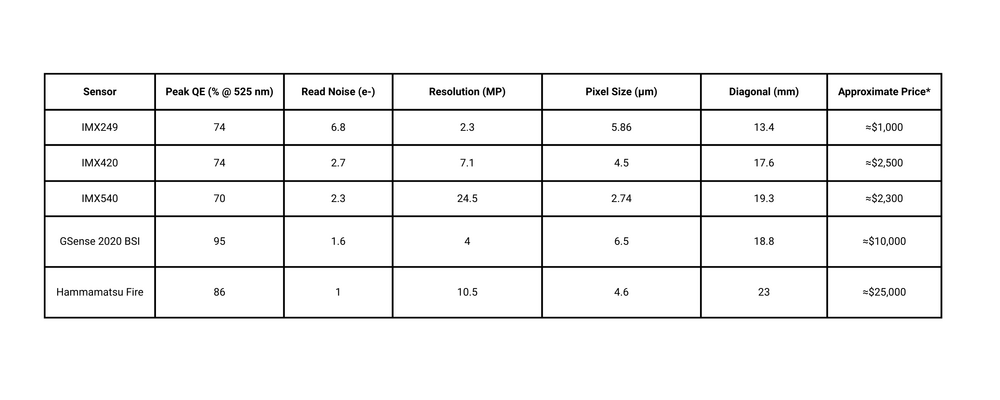
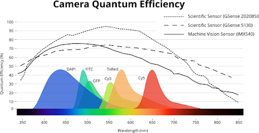
The small size, integration-friendly features and cost effectiveness of machine vision cameras make them an attractive option for OEM devices where minimizing the device footprint and retail price are important considerations. How are machine vision cameras different from scientific cameras? The distinction between machine vision and scientific cameras is not as clear as it once was. The term “Scientific CMOS” (sCMOS) was introduced in the mid 2010’s as advancements of CMOS image sensor technology lead to the development of the first CMOS image sensor cameras that could challenge the performance of then-dominant CCD image sensor technology. These new “sCMOS” sensors delivered improved performance relative to the CMOS sensors that were prevalent in MV cameras of the time. Since then, thanks to the rapid pace of CMOS image sensor development, the current generation of MV oriented CMOS sensors boast impressive performance. There are now many scientific cameras with MV sensors, and many MV cameras with scientific sensors.


Sunday, June 15, 2025

Conference List - December 2025

18th International Conference on Sensing Technology (ICST2025) - 1-3 December 2025 - Utsunomiya City, Japan - Website

International Technical Exhibition on Image Technology and Equipment (ITE) - 3-5 December 2025 - Yokohama, Japan - Website

7th International Workshop on New Photon-Detectors (PD2025) - 3-5 December 2025 - Bologna,, Italy - Website

IEEE International Electron Devices Meeting - 6-10 December 2025 - San Francisco, CA, USA - Website


If you know about additional local conferences, please add them as comments.

Return to Conference List index

Friday, June 13, 2025

Videos of the day: UArizona and KAIST


UArizona Imaging Technology Laboratory's sensor processing capabilities


KAIST  Design parameters of freeform color splitters for image sensors

Thursday, June 12, 2025

Panasonic single-photon vertical APD pixel design

In a paper titled "Robust Pixel Design Methodologies for a Vertical Avalanche Photodiode (VAPD)-Based CMOS Image Sensor" Inoue et al. from Panasonic Japan write:

We present robust pixel design methodologies for a vertical avalanche photodiode-based CMOS image sensor, taking account of three critical practical factors: (i) “guard-ring-free” pixel isolation layout, (ii) device characteristics “insensitive” to applied voltage and temperature, and (iii) stable operation subject to intense light exposure. The “guard-ring-free” pixel design is established by resolving the tradeoff relationship between electric field concentration and pixel isolation. The effectiveness of the optimization strategy is validated both by simulation and experiment. To realize insensitivity to voltage and temperature variations, a global feedback resistor is shown to effectively suppress variations in device characteristics such as photon detection efficiency and dark count rate. An in-pixel overflow transistor is also introduced to enhance the resistance to strong illumination. The robustness of the fabricated VAPD-CIS is verified by characterization of 122 different chips and through a high-temperature and intense-light-illumination operation test with 5 chips, conducted at 125 °C for 1000 h subject to 940 nm light exposure equivalent to 10 kLux. 


Open access link to full paper:  https://www.mdpi.com/1424-8220/24/16/5414

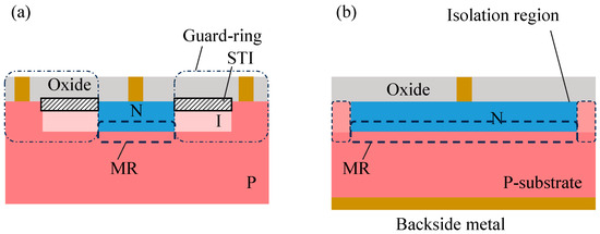
Cross-sectional views of a pixel: (a) a conventional SPAD and (b) a VAPD-CIS. N-type and P-type regions are drawn by blue and red, respectively.
 

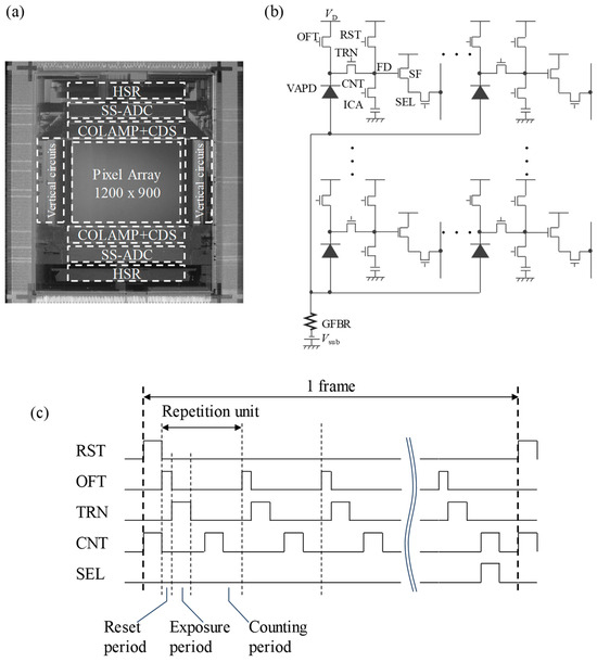
(a) A chip photograph of VAPD-CIS overlaid with circuit block diagrams. (b) A circuit diagram of the VAPD pixel array. (c) A schematic timing diagram of the pixel circuit illustrated in (b).
 
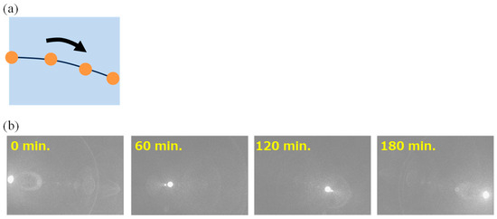
(a) An illustrative time-lapsed image of the sun. (b) Actual images of the sun taken at each time after starting the experiment. The test lasted for three hours, and as time passed, the sun, initially visible on the left edge of the screen, moved to the right.

Monday, June 09, 2025

Image Sensor Opening at Apple in Japan

Apple Japan

Image Sensor Technical Program Manager - Minato, Tokyo-to, Japan - Link

Friday, June 06, 2025