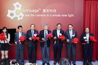
InVisage has inaugurated its first high-volume, fully automated QuantumFilm sensor manufacturing facility in Hsinchu Science Park, Taiwan. “After a review of various U.S. and Asian locations, we chose to establish our high-volume manufacturing in Taiwan because of the vitality of the semiconductor ecosystem here, and in particular because of our partnership with TSMC,” said InVisage’s CEO, Jess Lee. “Thanks to our high-calibre engineering and manufacturing staff here, we were able to source and install custom, state-of-the-art fabrication equipment and are now well positioned to ramp up QuantumFilm production.”
The manufacturing facility, called QFAB3, is said to feature an unprecedented sub-5nm process geometry within an ISO Class 10 cleanroom. It is designed to support a wide range of products, from mobile phones to high-end cameras as well as drones and other IoT devices that require high performance cameras.
“Because we use quantum dots, we don’t need finely patterned lithography to achieve our high performance and sub 5-nm scale. This QuantumFilm fab has a multiplier effect in terms of product performance, value, and output. So our factory is compact and accomplishes much more than the typical fab,” said James Chou, VP of Manufacturing Operations. “All the steps could fit within one shipping container. This enables many expansion opportunities we’re already scouting for.”
InVisage’s product wafers are first manufactured by nearby TSMC and then transferred to QFAB3 for QuantumFilm deposition. The deposition itself is performed by a single, custom tool that combines spin-coating and CVD deposition technologies into one machine for the first time. This combination allows the deposition process to be both modular and fully automated. This is said to be the first of many facilities to come as InVisage increases its capacity aiming to QuantumFilm technology to become the new standard for cameras.

What means sub-5nm Fab?? I'm afraid that this becomes the biggest joke in imaging industry one day.
ReplyDeleteNeedless to say, foundry's best partner is a fabless company.
ReplyDeleteNow that OVT was bought by China,
Nobel InVisage is absolutely the best tsmc's partner.
Noticeable tsmc resources will be spent into them.
Oh the spin makes my head spin. 5nm fab.... Pllllease... Reminds me of Signals decision to market Foveon as a sensor at 3x higher effective resolution. If invisage was selling iPhones to the great unwashed that may actually fly.
ReplyDelete....agreed: "we we don’t need finely patterned lithography to achieve sub 5-nm scale." Is this like CMOS claiming it has achieved 25 Ang scale without patterned litho because of the gate oxide thickness?
ReplyDelete