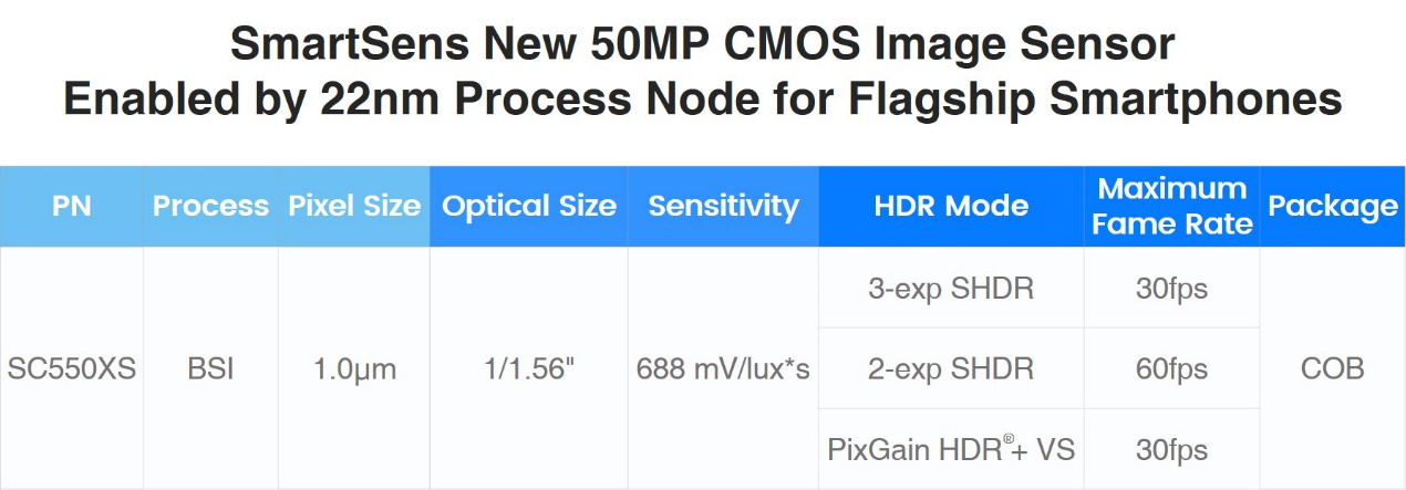
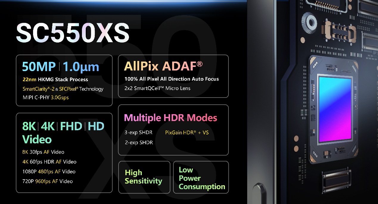
SmartSens has launched an ultra high resolution image sensor based on a 22nm process. SC550XS is their first 50MP ultra-high resolution image sensor with a 1.0μm pixel size. The new product adopts the advanced 22nm HKMG Stack process as well as SmartSens’ multiple proprietary technologies, including SmartClarity®-2 technology, SFCPixel® technology and PixGain HDR® technology to enable excellent imaging performance. In addition, it can achieve 100% all pixel all direction auto focus coverage via AllPix ADAF® technology and is equipped with MIPI C-PHY 3.0Gsps high-speed data transmission interface. The product is designed to address the requirements of flagship smartphone main camera in terms of night vision full-color imaging, high dynamic range, and low power consumption.

Full press release: https://www.smartsenstech.com/en/page?id=179


Apparently this is a stacked device, and a technology node of 22 nm is claimed. Is the 22 nm the technology node for the top layer (= light sensitive part), for the bottom layer (= processing part) or for both ? This is not really clear from the press release.
ReplyDeleteDon't know for sure, but similarly to Sony/Samsung/OmniVision I would think they are using the 22nm technology node for the bottom layer.
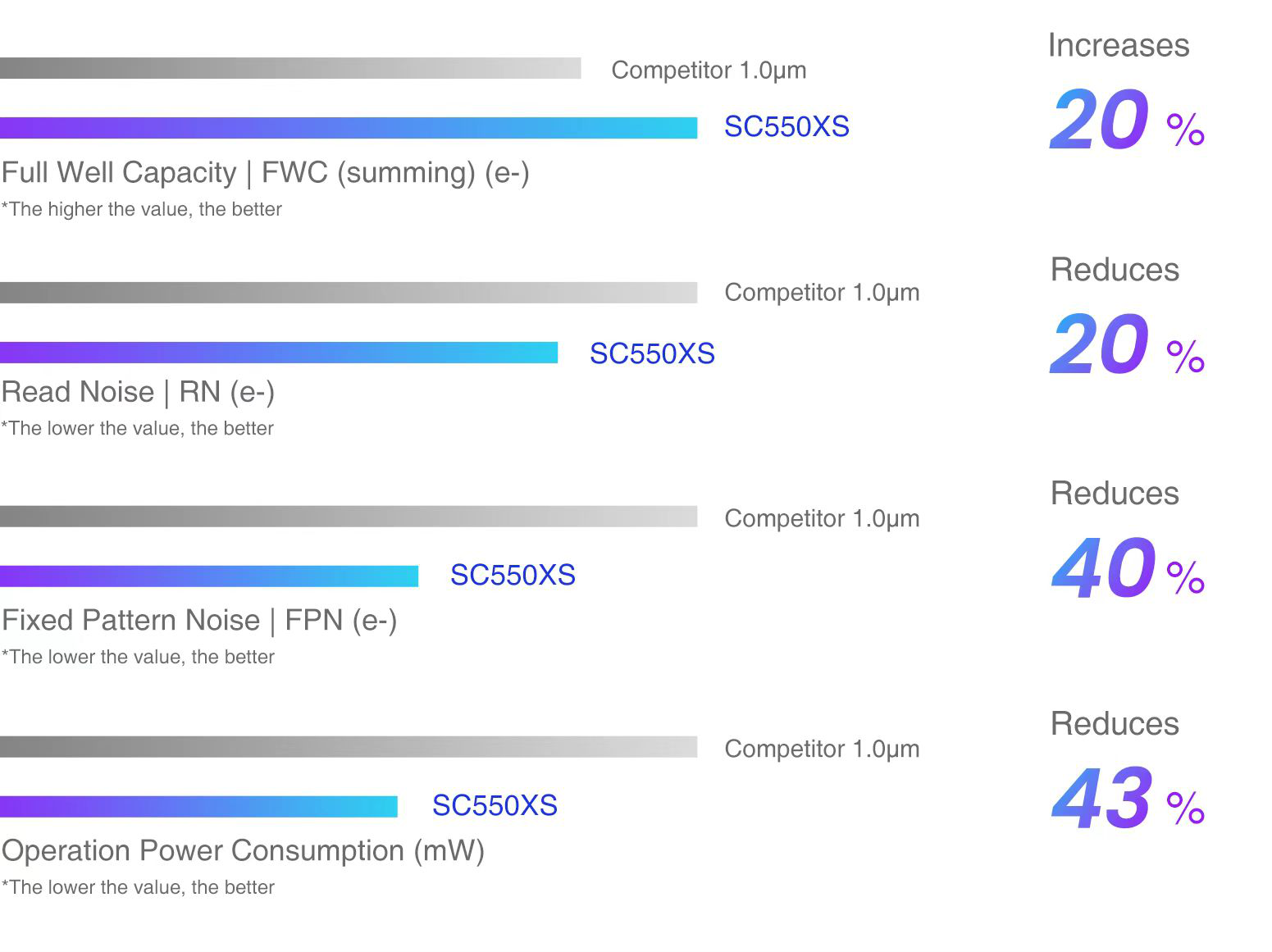
ReplyDeleteIt would be more helpful if they show number, rather than saying 20% increase, 20% reduction.
ReplyDeleteI already complained a hundred times about this, but it does not help ....
Delete