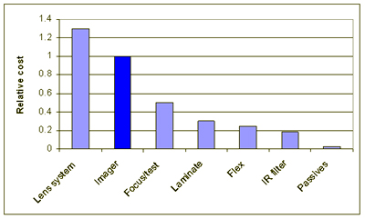
A relative costs chart for 1.3MP camera-phone module components from the article:

Article has an interesting claim concerning image sensor wafer thickness:
For conventional semiconductors, the industry is moving toward ever thinner die. Wafers are now routinely thinned to 75µm thickness, and even 25µm is being practiced in high-volume manufacture. The underlying advances in wafer thinning technology have enabled some of the remarkably slim format products and electronics accessories that are now available. Notable examples are flash memory cards, smart credit cards and the complexity of functionality that can now be crammed into USB devices.
By comparison, CMOS image sensors appear to be stuck in the Dark Ages with die thicknesses of hundreds of microns. There are two good reasons for this. The first is that the depth of black color (i.e. absence of light) that an imager is able to detect is determined by the leakage current of the photodiodes and certain active devices in the imaging array. This property is known as the "dark current" and can be measured. As a general rule, the dark current will increase as the semiconductor wafer thickness diminishes, and hence this metric affects the low light performance of the camera.
The second consideration is mechanical. When the glass cover is attached to the imager, the center region of the die is provided with mechanical reinforcement. This leaves vulnerable protruding ledges where the bond pads are located. If the die is too thin, the fragility of these ledges is reflected in manufacturing yield loss.
No comments:
Post a Comment
All comments are moderated to avoid spam and personal attacks.