NHK Broadcast Technology Magazine No.55, Winter 2014 presents a CIGS-based "photoconductive film capable of multiplying the original charges generated by the incident light by many times simply with a low applied voltage" which can be deposited on top of image (charge) sensor to improve its low-light sensitivity:
The feature article talks about the progress in 8K UHDTV image sensors:
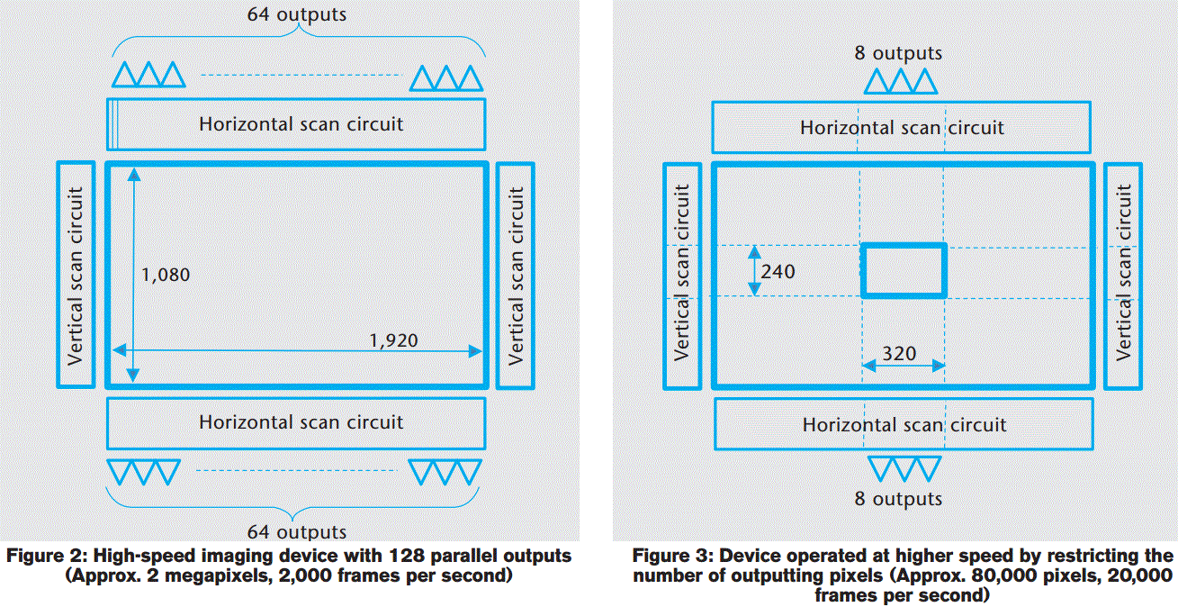
Another feature article talks about NHK R&D on high speed image sensors. "It is currently possible to purchase a monochrome camera with a resolution of 100,000 pixels that can capture video at up to ten million frames per second."


Is this the continued work of their HARP sensor ?
ReplyDelete-yang ni
Sort of. HARP was a tube-based image sensor. NHK has been looking at stacked structures as part of their Amplified MOS Imager (AMI) research for a long time and I think they looked at a-Se overlayers (which are the basis for Super HARP tubes) already. The CIGS is a newer thrust I believe.
DeletePersonally, I think this would be very interesting for the QIS, where gain control is less important, and pixel size reduction may be easier to achieve than in SPADs.
I remember that Super HAD was not based on tube technology. it was based on avalanching mechanism inside the photo sensing layer.
Delete-yang ni
Yes, but only implemented successfully with tubes. It is a tube technology.
DeleteThanks Eric ! I didn't know this. So why in tubes ? Some material stability problems ?
Delete-yang ni
You would think that the coating would work equally well on tubes and solid-state devices. I don't recall hearing about success with solid-state devices but I know they were working on it. I will ask some of my NHK friends about it.
DeleteAh! it could be the deposition temperature for the thin tim. Indeed many tube based solutions are very powerful, high sensitivity and very low dark current, but unfortunately high temperature deposition is needed, which is not compatible with CMOS active wafers.
Delete-yang ni
It would be interesting to know how large are dark current and avalanche multiplication noise in this technology
ReplyDeleteLucio Pancheri