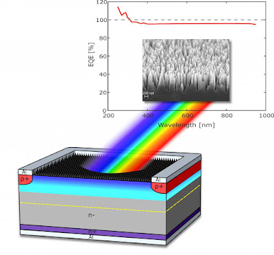
Opli quotes Nature Photonics paper "Near-unity quantum efficiency of broadband black silicon photodiodes with an induced junction" by Mikko A. Juntunen, Juha Heinonen, Ville Vähänissi, Päivikki Repo, Dileep Valluru & Hele Savin from Aalto University, Espoo, Finland. From the abstract:
"Present-day photodiodes notably suffer from optical losses and generated charge carriers are often lost via recombination. Here, we demonstrate a device with an external quantum efficiency above 96% over the wavelength range 250–950 nm. Instead of a conventional p–n junction, we use negatively charged alumina to form an inversion layer that generates a collecting junction extending to a depth of 30 µm in n-type silicon with bulk resistivity larger than 10 kΩ cm. We enhance the collection efficiency further by nanostructuring the photodiode surface, which results in higher effective charge density and increased charge-carrier concentration in the inversion layer. Additionally, nanostructuring and efficient surface passivation allow for a reliable device response with incident angles up to 70°."
Thanks to TG for the link!


What is the dark current?
ReplyDeleteWhat is new?
ReplyDeleteNot much. First, now Finland becomes the second source for black silicon devices. Second, they claim to create an inversion layer on the black silicon surface.
DeleteCould you please explain how the EQE is greater than 100% for wavelength < ~ 300nm?
ReplyDeleteHigh energy photons may excite more than one electron.
DeleteMost likely they did not correctly adjust for the absorbtion of the Al2O3 layer itself.
DeleteAl2O3 has bandgap of around 7.6 eV and does not absorb wavelength >200 nm.
Delete