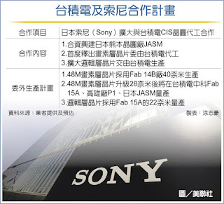
It is reported that Sony plans to use the 40nm process of TSMC's Nanke Fab 14B plant for its 48-megapixel layer chip, and will upgrade and expand the use of the 28nm mature special process in the future. factory, as well as the joint venture fab JASM in Kumamoto, Japan.
In addition, the logic layer chip at the core of Sony's ISP will also be handed over to TSMC for mass production, using the 22nm process of China's Fab 15A, but the color filter film and microlens process in the latter stage will still be shipped to Sony's own factory in Japan. completed within.
Regarding Sony's change in attitude, the industry believes that this is mainly to meet the demand for the iPhone 14 equipped with a 48-megapixel CMOS image sensor for the first time."

No comments:
Post a Comment
All comments are moderated to avoid spam and personal attacks.