1.5µm dual conversion gain, backside illuminated image sensor using stacked pixel level connections with 13ke- full-well capacitance and 0.8e- noise
V. C. Venezia, A. C-W Hsiung, K. Ai, X. Zhao, Zhiqiang Lin, Duli Mao, Armin Yazdani, Eric A. G. Webster, L. A. Grant, OmniVision Technologies
Omnivision presented two stacked designs with pixel-level interconnects. Design A has been selected as a more optimal from the DR point of view:


A 0.68e-rms Random-Noise 121dB Dynamic-Range Sub-pixel architecture CMOS Image Sensor with LED Flicker Mitigation
S. Iida, Y. Sakano, T. Asatsuma, M. Takami, I. Yoshiba, N. Ohba, H. Mizuno, T. Oka, K. Yamaguchi, A. Suzuki, K. Suzuki, M. Yamada, M. Takizawa, Y. Tateshita, and K. Ohno, Sony Semiconductor
Sony presented its version of Big-Little PDs in a single pixel:


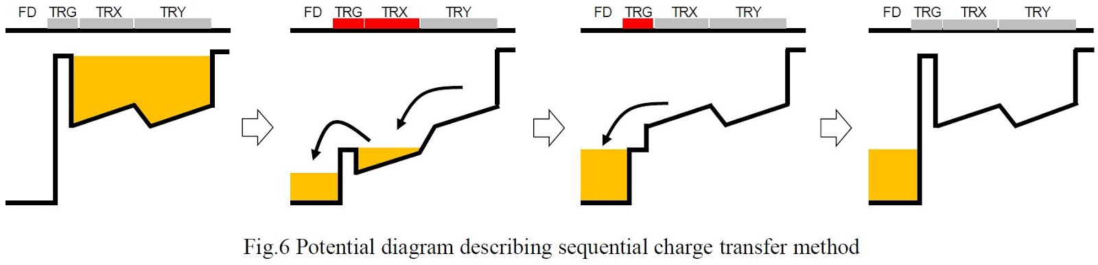
A 24.3Me- Full Well Capacity CMOS Image Sensor with Lateral Overflow Integration Trench Capacitor for High Precision Near Infrared Absorption Imaging
M. Murata, R. Kuroda, Y. Fujihara, Y. Aoyagi, H. Shibata*, T. Shibaguchi*, Y. Kamata*, N. Miura*, N. Kuriyama*, and S. Sugawa, Tohoku University, *LAPIS Semiconductor Miyagi Co., Ltd.
Tohoku University and LAPIS present an evolution of their LOFIC pixel with deeply depleted PDs on 1e12 cm-3 doped substrate:


HDR 98dB 3.2µm Charge Domain Global Shutter CMOS Image Sensor (Invited)
A. Tournier, F. Roy, Y. Cazaux*, F. Lalanne, P. Malinge, M. Mcdonald, G. Monnot**, N. Roux**, STMicroelectronics, **CEA Leti, **STMicroelectronics
ST and Leti explain their dual memory pixel architecture:


High Performance 2.5um Global Shutter Pixel with New Designed Light-Pipe Structure
T. Yokoyama, M. Tsutsui,Y. Nishi, I. Mizuno, V. Dmitry, A. Lahav, TPSCo & TowerJazz
TowerJazz and TPSCo show their latest generation small GS pixel available for the foundry customers:


Back-Illuminated 2.74 µm-Pixel-Pitch Global Shutter CMOS Image Sensor with Charge-Domain Memory Achieving 10k e- Saturation Signal
Y. Kumagai, R. Yoshita, N. Osawa, H. Ikeda, K.Yamashita, T. Abe, S. Kudo, J. Yamane, T. Idekoba, S. Noudo, Y. Ono, S.Kunitake, M. Sato, N. Sato, T. Enomoto, K. Nakazawa, H. Mori, Y. Tateshita, and K. Ohno, Sony Semiconductor
Sony presented its approach to shielding the storage nodes in BSI GS sensor:


Hi Vladimir,
ReplyDeleteis it possible to download the papers somewhere?
The only official option is at IEEE site in a couple of months from now.
DeleteFor the Big-Little PDs in Sony`s 121dB DR pixel, how the noise performance when they transition from big to small. Will that be an issue ?
ReplyDeleteThe SNR drops from 40dB to ~22dB on the transition. There is a graph in the paper showing that.
Delete22dB ... do you consider that good or bad?
DeleteIt is what it is... At least, Sony openly presents the data so that everybody can decide.
DeleteIn OVT's paper, the pixel level interconnect is part of the FD and might contribute considerably to the PRNU. Is there any PRNU value in the papers? I think that is the main issue of such approach.
ReplyDeleteThere is no PRNU data in the paper.
Delete