In a recent paper titled "Achieving higher photoabsorption than group III-V semiconductors in ultrafast thin silicon photodetectors with integrated photon-trapping surface structures", Qarony et al. from UC Davis, W&Wsens Devices Inc. and UC Santa Cruz write:
The photosensitivity of silicon is inherently very low in the visible electromagnetic spectrum, and it drops rapidly beyond 800 nm in near-infrared wavelengths. We have experimentally demonstrated a technique utilizing photon-trapping surface structures to show a prodigious improvement of photoabsorption in 1-μm-thin silicon, surpassing the inherent absorption efficiency of gallium arsenide for a broad spectrum. The photon-trapping structures allow the bending of normally incident light by almost 90 deg to transform into laterally propagating modes along the silicon plane. Consequently, the propagation length of light increases, contributing to more than one order of magnitude improvement in absorption efficiency in photodetectors. This high-absorption phenomenon is explained by finite-difference time-domain analysis, where we show an enhanced photon density of states while substantially reducing the optical group velocity of light compared to silicon without photon-trapping structures, leading to significantly enhanced light–matter interactions. Our simulations also predict an enhanced absorption efficiency of photodetectors designed using 30- and 100-nm silicon thin films that are compatible with CMOS electronics. Despite a very thin absorption layer, such photon-trapping structures can enable high-efficiency and high-speed photodetectors needed in ultrafast computer networks, data communication, and imaging systems, with the potential to revolutionize on-chip logic and optoelectronic integration.
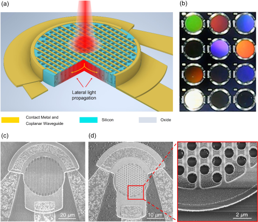
Design and fabrication of highly absorbing thin-film Si photon-trapping photodetector. (a) Schematic of the photon-trapping silicon MSM photodetector. The photon-trapping cylindrical hole arrays allow lateral propagation by bending the incident light, resulting in an enhanced photon absorption in Si. (b) Optical microscopy images of the photon-trapping photodetectors fabricated on a 1 μm thin Si layer of the SOI substrate for a range of hole diameters, d, and period, p of the holes. Under white light illuminations, the flat devices look white (bottom left) because of surface reflection. The most effective photon-trapping device looks black (bottom right). Less effective photon-trapping devices show different colors reflected from the surface of the devices. SEM images of fabricated (c) planar and (d) photon-trapping MSM photodetectors. The inset indicates circular-shaped holes in a hexagonal lattice formation (Video 1, mp4, 5.27 MB [URL: https://doi.org/10.1117/1.APN.2.5.056001.s1]).
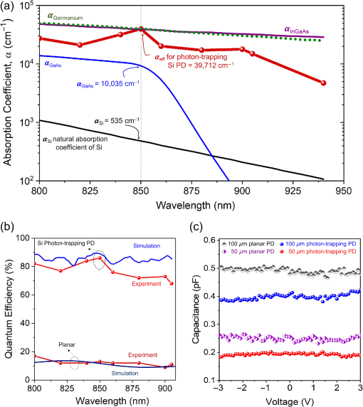
Experimental demonstration of absorption enhancement in Si that exceeds the intrinsic absorption limit of GaAs. (a) Comparison of the enhanced absorption coefficients (αeff) of the Si photon-trapping photodetectors and the intrinsic absorption coefficients of Si (bulk),57 GaAs,57 Ge,56 and In0.52Ga0.48As.56 The absorption coefficient of engineered photodetectors (PD) shows an increase of 20× at 850 nm wavelength compared to bulk Si, exceeds the intrinsic absorption coefficient of GaAs, and approaches the values of the intrinsic absorption coefficients of Ge and InGaAs. (b) The measured quantum efficiencies of the Si devices have an excellent agreement with FDTD simulation in both planar and photon-trapping devices. (c) Photon-trapping photodetectors exhibit reduced capacitance compared to their planar counterpart, enhancing the ultrafast photoresponse capability of the device (Video 2, mp4, 9.68 MB [URL: https://doi.org/10.1117/1.APN.2.5.056001.s2]).
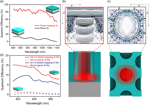
Theoretical demonstration of enhanced absorption characteristics in ultrathin Si film integrated with photon-trapping structures. (a) Comparison of simulated absorption of photon-trapping [Fig. 1(a) and Fig. S7 in the Supplementary Material] and planar structures demonstrates absorption efficiency in photon-trapping Si around 90% in 1 μm thickness. In contrast, the black curve shows extremely low-absorption efficiency in planar Si without such surface structures. Calculated Poynting vectors in holey 1 μm thin Si on (b) x−z (cross section) and (c) x−y (top view) planes showing that the vectors originated from the hole and moved laterally to the Si sidewalls, where the photons are absorbed. (d) Simulated enhanced optical absorption in ultrathin Si of 30 and 100 nm thicknesses with and without photon-trapping structures.
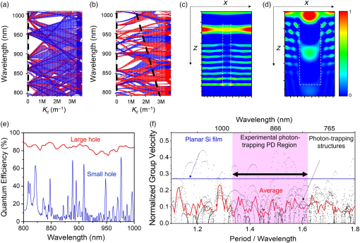
Reduced group velocity in photon-trapping Si (slow light) and enhanced optical coupling to lateral modes contribute to enhanced photon absorption. Calculated band structure of Si film with (a) small holes (d=100 nm, p=1000 nm, and thickness, tSi=1000 nm) and (b) large holes (d=700 nm, p=1000 nm, and thickness, tSi=1000 nm). Red curves represent TE modes and blue curves represent TM modes. Slanted dashed lines are solutions for kc that couple into the lateral propagation for a vertically illuminating light source. Small hole structures exhibit solutions only for the finite number of the eigenmodes with k=0 (vertical dashed line), whereas large hole structures essentially have both solutions k=kc and k=0 (vertical and slanted dashed lines) with the eigenmodes, pronouncing enhanced coupling phenomena and laterally propagated optical modes. (c) FDTD simulations exhibit optical coupling and the creation of lateral modes. Low coupling and photonic bandgap phenomena are observed for the hole size smaller than the half-wavelength. (d) Larger holes that are comparable to the wavelengths of the incident photons facilitate a higher number of optical modes and enhanced lateral propagation of light. (e) Calculated optical absorption in Si with a small hole (d=100 nm, p=1000 nm, and thickness, tSi=1000 nm) compared with the absorption of the large hole (d=700 nm, p=1000 nm, and thickness=1000 nm). (f) For frequencies (period of holes/light wavelength) between 1.3 and 1.6, the normalized light group velocity (red curve) for 850 nm wavelength is significantly lower in photon-trapping Si compared to that of the bulk Si (blue line). The red curve represents an averaged group velocity for Si photon-trapping structures, which exhibits a distinctly lower value in our fabricated devices (Video 3, mp4, 12.4 MB [URL: https://doi.org/10.1117/1.APN.2.5.056001.s3]).
No comments:
Post a Comment
All comments are moderated to avoid spam and personal attacks.